A related question is a question created from another question. When the related question is created, it will be automatically linked to the original question.
If you have a related question, please click the "Ask a related question" button in the top right corner. The newly created question will be automatically linked to this question.
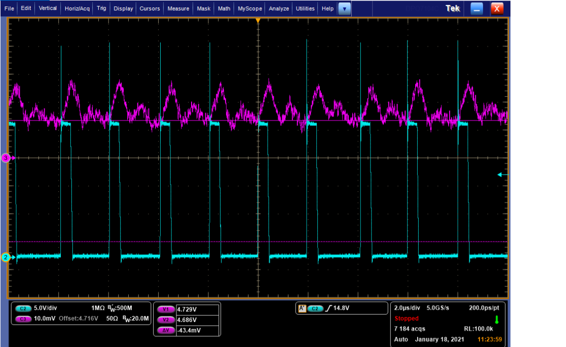
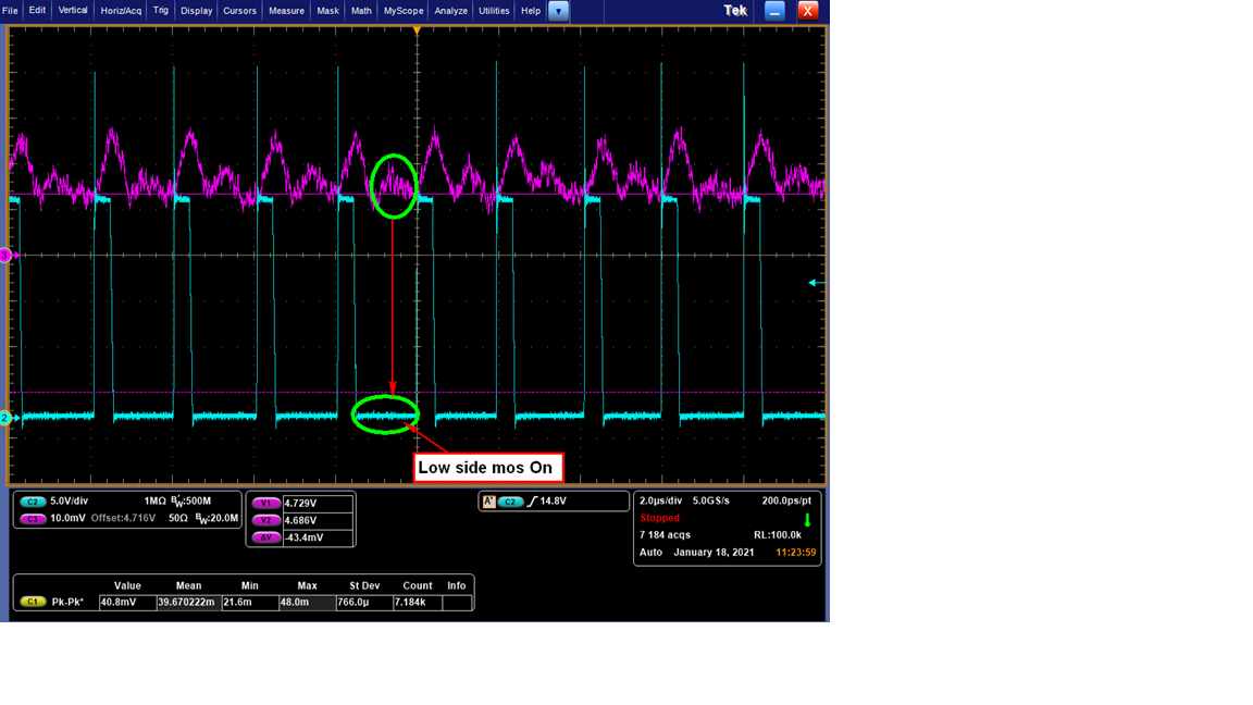
The initial spike on the rising edge of the switching node appears to be high, suggesting that that Power Input bypassing could be improved, or a snubber used, and the spike amplitude should be compared against the break-down voltage rating of the low-side FET, and the output voltage ripple suggests that there may be a 1MHz inter-capacitance resonant frequency, but I do not see anything particularly bad about the waveforms, just a few minor improvements that could be made.
As I pointed out in my prior e-mail, there appears to be an approximately 1MHz inter-capacitance resonance in the output capacitor bank. The ESL and layout inductance between two ceramic capacitors of different values is creating a resonant tank. This is not uncommon when smaller capacitors with 10:1 capacitance ratio are used to lower the output impedance at high frequency. For 1MHz, a common capacitor pair would be 10uF and 1.0uF.
If the small amount of 1MHz ripple needs to be suppressed, you can try adding a 3.3uF capacitor between the 10uF and 1.0uF to reduce the impedance in between the two capacitors self-resonance frequencies.