


Hi,
We are using TPS65266-1 in our design to generate 1.5v, 1v & 1.8v.
Attaching the schematics. Please review and let us know if the discrete values at each output are correct.
L8, L9, & L10 value-2.2uH
Thanks,
Tejaswi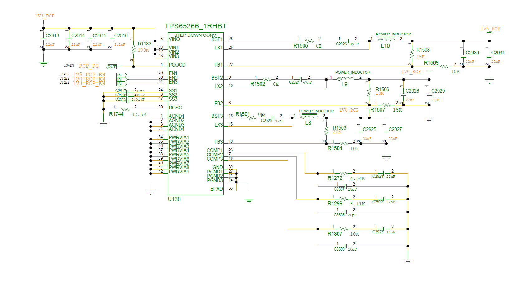
Hi,
We are using TPS65266-1 in our design to generate 1.5v, 1v & 1.8v.
Attaching the schematics. Please review and let us know if the discrete values at each output are correct.
L8, L9, & L10 value-2.2uH
Thanks,
Tejaswi
