This thread has been locked.

If you have a related question, please click the "Ask a related question" button in the top right corner. The newly created question will be automatically linked to this question.

LM5106: no dead time in half bridge at Vds high side and low side

Part Number: LM5106

Hi 

I have an half bridge which is driven by LM5106.

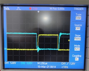
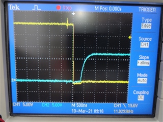
I have around 400nS dead time between high side and low side Vgs. But there is no effect of the this dead time at Vds for high side and low side mosfet.

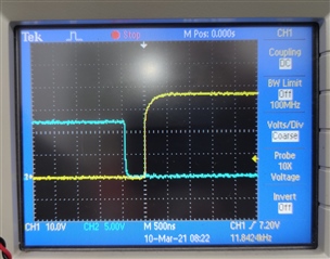
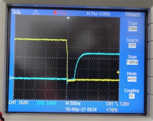
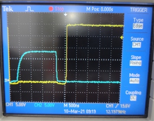
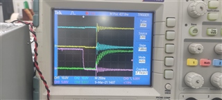
As you can see in the picture CH3 (Green) and CH4 (Purple) are Vgs high side and Vgs low side. 

* the noise is because of the wiring to the oscilloscope *

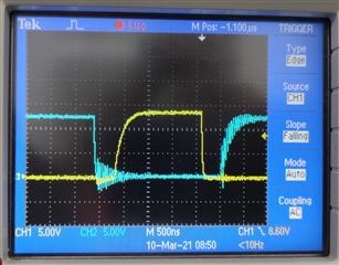
CH1 (Yellow) is drain source voltage of the high side mosfet and CH2 (Blue) is drain source voltage of the low side mosfet.


even if I unplug the motor the signals are exactly the same.

this switching without dead time is happening in few nS but still effect on the DC line and motor current.

I already played with Rdt and increased the dead time but it is still the same Vds high side and low side change together.

the schematic is same with LM5106 schematic recommended in the datasheet

I need to know what is the reason of this problem that I have.

  • Hello Morteza,

    Thank you for the interest in the LM5106. The dead time will be from the LO and HO driver outputs rising/falling edges but depending on the power train condition, the MOSFET Vds may still transition after the conducting MOSFET turns off, and not necessarily when the other bridge FET turns on.

    Can you confirm the timing of the LO and HO outputs to see if there is the expected dead time? Also confirm the timing of the switch node, HS, waveform relative to the LO and HO driver signals.

    If the power MOSFET switch node is transitioning early, before expected, this is not harmful and is dependent on the power train current flowing.

    Confirm if this addresses your concerns or you can post additional questions on this thread.

    Regards,

  • Hello Richard 

    Thanks for your reply.

    the picture bellow is LO and HO out put of the IC LM5106 to GND:

    CH1 (yellow) is HO and CH2 (Blue) is LO.

    So the dead time is exactly correct correct and is 400nS. although sometimes is smaller duty cycle in input pwm (25KHz) the HO is not that clean, you can see in this picture:

    but when I check HO to HS and LO to GND, the dead-time and the waveform are always clean and perfect:

    **So I am sure that the High side and Low side gate source voltages are good with the correct 400nS dead-time that I want.**

    the problem is as I mentioned before, the Vds or both MOSFETs drain-source voltages are switching at the same time and when I check the DC line voltage and current I have spikes exactly at the moment that those high side and low side mosfets are switching. 

    I was expecting that the drain source voltage follow the Vgs but I see that it is not like this.

    for example the picture below shows gate-source and drain-source voltage for low side mosfet. 

    this picture clearly shows that Vds turned ON before I turn on the Gate source voltage.

    or for the high side mosfet I can show this picture that shows the drain source voltage not really follows the gate source voltage:

    I need to know the reason.

    Regards.

  • Hello Morteza,

    Thank you for the additional scope plots, which confirm as you mention that he driver HO and LO outputs are behaving as expected regarding the dead time.

    If there is positive current flowing in the power train, usually in the inductance to the load, which is always above zero including peak to peak ripple current, when the high side switch turns off, the positive current that is flowing in the output will force the polarity across the inductor to reverse which results in the Vds falling and the current in the power train to conduct in the low side switch body diode. The low side Vds will be low even before the low side FET turns on in this case. Also in many cases when you turn off the low side FET the VDS stays low, until the high side FET turns on. So the VDS may follow the high side turn on edge, but also fall on the high side FET turn off edge.

    I am not sure in your circuit that you can change this behavior in the power train, it is a function of the output load, switching frequency and inductance. Many converters operate in this way, under certain load conditions with no issues other than some power dissipation from the FET body diode conduction.

    Confirm if this addresses your questions, or you can post additional questions on this thread.

    Regards,

  • Hello Richard 

    Thanks for the info sharing with me.

    This was the answer of of my question.

    Regards.