- Ask a related questionWhat is a related question?A related question is a question created from another question. When the related question is created, it will be automatically linked to the original question.
Hi everybody,
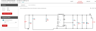
i intent to use the LMZM33603 as in inverter to get -10V from a 24V source.
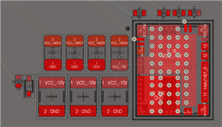
Power designer gives me the proposed design, which translates into the PCB as shown.
but as now the normally indented GND and VCC pins are swapped, it generates different path for the input and output caps.
do you still think this is the correct placement for a good EMI performance, or should we change it?
would be great to get some insights.
Fabian