This thread has been locked.

If you have a related question, please click the "Ask a related question" button in the top right corner. The newly created question will be automatically linked to this question.

TPS543B20: Ramp resistor selection

Part Number: TPS543B20

Hello,

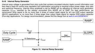
Some colleagues recently measured the loop gain on a TPS543B20 based buck converter using five different ramp resistor selections and found 34.8k to be the best in terms of worst case phase margin. However, we would like to understand why this particular ramp resistor is the optimal selection and what it’s role is in the control scheme of the component so that this is not just a trial & error approach to optimization. 

The application parameters are as follows:

  • Vin = 12 V (10.4 V - 14 V range)
  • Vout = 2.5 V
  • Iout = 18 A max
  • Cout = 230 uF
  • L = 400 nH

The results were as follows:

Phase Margin(°margin)

Resistor

None

23.7k

34.8k

51.1k

78.7k

14V,18A

43.99

46.7

47.7

45.7

34.3

12V,18A

45.507

51.1

53.15

48.9

45

10.4V,18A

47.182

53.9

55.1

58.9

54.3

14V,8.6A

41.887

49.8

51.9

52.9

50.4

12V,8.6A

43.323

53.4

56.4

58.7

55.9

10.1V,18A

46.192

56.1

59.6

64.5

65.2

Bandwidth

Resistor

None

23.7k

34.8k

51.1k

78.7k

14V,18A

122.9

179.2

190.1

249.6

306.8

12V,18A

120.4

179.9

191.8

249.6

247.7

10.4V,18A

111

161.3

172.7

215.8

230.6

14V,8.6A

152.2

142.7

149.3

184.2

209.9

12V,8.6A

147.8

144.6

154.3

189.3

249.7

10.1V,18A

134.8

133.2

139.4

171

206.2

Any clarification would be appreciated.

Thank you,

Nick

  • Hi

        Decreasing the ramp resistor, lowers the internal ramp capacitor. So the ramp slope increases. As the ramp slope increases, a small change in Vout/FB voltage will only change the duty cycle by a small amount. This means that gain is small. If gain is small, then cross over will happen soone, which means phase will be high.

    Hope this helps.

    regards,

    Gerold

  • Hi Gerold,

    Thank you for that explanation. That definitely clears up that this ramp slope is the injected artificial ramp in a current mode controlled buck converter that prevents instability for duty cycle larger than 0.5, and how the ramp slope amplitude affects the loop gain of a current mode controlled buck converter in general.

    Turning to the TPS543B20, section 8.4.6 of the datasheet describes how the artificial ramp is generated. In this section there is a recommendation to set the "ramp signal to be no more than 4 times of output ripple signal" for low ESR output capacitors like in our application.

    1) I'm curious what the circuit, and accompanying equation, to calculate the slope of this ramp signal given the RC circuit. Is it a simple RC series circuit being charged by the internal linear regulator? This seems important as it's important to choose the ramp slope relative to the emulated inductor current ripple in this part.

    2) Where does the recommendation that relates the ramp slope to the output ripple come from? The output voltage ripple relates to the inductor ripple approximately by

    However, the controller has no way of knowing the amount of output capacitance on the rail, and so this recommendation seems dependent on implementation.

    Any clarification on these two points would be greatly appreciated.

    Nick

  •  

    0) The TPS543x20 family of parts do no sense the inductor current through the switching cycle,  They collect average inductor current information from the low-side switch during the off-time, but the internally generated ramp is the only cycle by cycle ramp used for the internal control.  It must represent both the cycle by cycle inductor ripple current plus the slope-compensation needed to maintain stable operation above 50% duty cycle.  Since the internal ramp is the sole ripple used for cycle by cycle PWM control, the effective current sense gain of the converter at cross-over is proportional to L/RC where L is the inductor value and R-C is the time constant of the internal ramp generator.

    1) The internal ramp is a simple R-C ramp driven by the internal BP regulator and pulse-width modulated by the same PWM signal that drives the power-FETs.

    2) The recommendation in the datasheet that the RC ramp amplitude should be no more than 4x the capacitive ripple on the output is an attempt to limit how large of a ramp is used, and the resulting total phase angle of the combined ripple coming into the TPS543x20 through the FB pin (capacitive ripple from the output voltage) and the emulated resistive ripple injected by the ramp generator.  When the capacitive ripple and the resistive ripple are equal in amplitude, the TPS543x20 will have approximately 45 degrees of phase margin.  As the emulated resistive ripple gets larger relative to the sensed capacitive ripple, the bandwidth decreases by the phase margin increases.  Limiting the resistive ripple to no more than 4x the capacitive ripple prevents the designer from using an excessively large ramp and thus achieving lower bandwidth.

    I am double checking on the detailed values of the internal ramp generator, and will include them here shortly.

  •  

    I looked up the details of the internal ramp generator earlier with design.

    The voltage source for the ramp generator is BP

    The resistor is 300kOhms

    There is a 20:1 gain stage in the circuit the makes the effective ramp 1/20 the value calculated by the RC.

    The forward transconductance from FB to Inductor Current is 20x ( Vin / Vbp ) x  (RC / L) 

    The loop will crossover at the frequency where resistor divider (Vout to FB) time the forward transconductance time the output impedance (Zout) is equal to zero.