This thread has been locked.

If you have a related question, please click the "Ask a related question" button in the top right corner. The newly created question will be automatically linked to this question.

BQ24171: About the maximum rating of the ISET terminal of BQ24171

Part Number: BQ24171

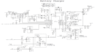
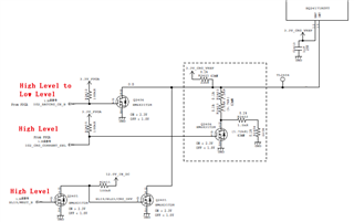
I have a question about the ISET terminal of BQ24171RGYT.

The "BQ24171RGYT" charging current setting terminal (ISET terminal) is switched from 0V to 120mV or more using FET, but once it is changed from 0V to 120mV or more, the voltage drops to around -400mV.

The schematic and waveform are attached.

CH1:ISET

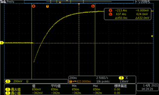
It seems that BQ24171RGY is pulling to -400mV.
Isn't there such a thing?
The maximum rating of the ISET terminal is stated as -0.3V in the data sheet. Is the maximum rating of the ISET terminal really -0.3V?

Please answer.

  • Hello,

    Can you please send a more detailed schematic with clearer part numbers, annotations, etc.? The resolution makes it hard to read the text. In addition, can you please indicate which path is being turned on or what sequence is happening when the voltage on the pin drops below -300 mV?

    Thanks,

    Mike Emanuel

  •  The circuit of the charge / discharge IC is attached.

    12.0V_IN_DC supplies 12.0V, and 3.3V_CRG_VREF outputs 3.3V.
    This is the waveform of TL2404 (ISET terminal) when the gate of Q2406-1 is changed from High to Low when the drain of Q2401-2 is in the OFF state and the drain of Q2406-2 is also in the OFF state.
    (When changing the drain of Q2406-1 from the ON state to the OFF state.)

    At this time, the voltage of the ISET pin falls below -300 mV.

  • Hello,

    I am having trouble understanding your logic. What do you mean the "drain of Q2401-2" is in the OFF state? Does that mean the FET is not conducting? If that is the case, if Q2401-2 is off then Q2401-1 is on through the pull-up, meaning that ISET is being pulled to ground the whole time. Please keep in mind you are driving it with 12 V. If the gate of Q2406-1 is changed from High to Low then that FET goes off, but the ISET node is still pulled to ground.

    Can you please send a detailed list of what you expect to happen, as well as measured voltages in each state? I am having trouble understanding your scheme.

    Thanks,

    Mike Emanuel

    Please click "Resolved" if this answered your question.

  • Excuse me. I made a mistake.

    When the drain is OFF, it means that it is not conducting with the source.
    When the drain is ON, it means that it is conducting with the source.

    Drain  of Q2401-2 was a mistake of ON.

    The gate of Q2401-2 is about 3.3V, and the gate of Q2401-1 is about 12V.
     Therefore, the drain of Q2401-1 is in the OFF state.
    The gate of Q2406-1 is about 3.3V, and the drain of Q2406-1 is ON, and the ISET terminal is conducting with GND. (Approximately 0 mV)

    From this state, the gate of Q2406-1 is changed to about 0V, and the moment the drain of Q2406-1 is turned off, the voltage of the ISET terminal drops below -300mV.
    After that, the voltage of the ISET pin rises to about 624 mV.

    Can you understand?

  • Hello,

    If the gate of Q2401-2 is 3.3V, its drain is ON and the drain is approximately 0 V. Therefore the gate of Q2401-1 is actually 0 V from the drain of Q2401-2 and Q2401-1 is off. Because the gate of the Q2406-1 is 3.3 V, its drain is on and ties ISET to ground. Driving the gate of Q2406-1 low would open the FET and the behavior of Q2406-2 would dominate the behavior.

    I am still having the trouble reading your schematic because the resolution is poor. Can you please send a schematic with clear text for components? If you have Q2401-1 off, what about Q2406-2? What is the expected final voltage you want to see?

    In addition, how far are these resistors/FETs from the pin? What is the trace width etc.?

    Thanks,

    Mike Emanuel

    Please click "Resolved" if this answered your question.

  • I don't know how to attach a file. Could you tell me.

    The operation of the circuit is correct.

    The gate of Q2406-2 is 0V and Q2406-2 is OFF.

    The pattern distance from the drain to the resistor of FET Q2406-1 is approximately 27mm.
    Is the trace width the time axis of the oscilloscope?
    If so, it is in the 200ns range.

    It takes about 100ns time to drop from 0V to about -392V and reach 0V or higher.

    Is the maximum rating of the ISET terminal really -0.3V?

  • Can you please confirm the operation of Q2401-2 and Q2401-1? They cannot be both conducting or both off, you have made an inverter out of them. Their states are designed to be opposite.

    I don't think you can attach a file. Please insert an image that has higher resolution that I can read. Please double check your post after upload to make sure all the text is visible.

    The trace width is how wide the copper is on its path from the pin to the resistors/FETs. The 27 mm you gave me is the trace length, which is the distance from the pin to the resistors/FETs along the copper.

    I need a very clear table from you which details the induced states of the FETs (inputs), the expected outcomes of the subsequent nodes (expected outputs), and the actual outcomes of the subsequent nodes (actual outputs). I do not understand the logic of what you are trying to do; having this information will help me debug the circuit.

    Yes, the absolute maximum rating of ISET is -0.3 V. This does not mean the pin will prevent itself from going below that voltage. Inducing the chip to have the ISET pin go below this voltage violates the maximum ratings and may cause permanent damage to the chip.

    Thanks,

    Mike Emanuel

    Please click "Resolved" if this answered your question.

  • The 2401-2 FET is ON, and the Q2401-1 FET is OFF.
    I will attach the schematic again.


    The minimum trace width is 0.1mm.

    It is a timing chart.

    Q2401-2 Q2401-1 Q2406-2 Q2406-1 Q2401-2 Q2401-1 Q2406-2 Q2406-1
    ON OFF OFF ON ON OFF OFF ON
    ISET=0V ISET=0.6V
  • Could not attach a high resolution image.

  • Hello,

    I really need a higher resolution image so I can see the resistors and transistors you are using. I typically use the Snipping Tool from Microsoft Windows and that works.

    In addition, I do not understand the operation table you gave me. The transistors in both states are exactly the same but yield different outcomes.

    Thanks,

    Mike Emanuel

  • I'm trying to paste an image with Snipping Tool, but I can't.
    (Currently, the image cannot be pasted by another method.)

    Since we have confirmed that the maximum rating of the ISET terminal is -0.3V, we will consider the circuit so that it does not fall below -0.3V for the ISET terminal.

    Thank you for your reply.

  • Is there anything else I can help with?

    Thanks,

    Mike Emanuel