This thread has been locked.

If you have a related question, please click the "Ask a related question" button in the top right corner. The newly created question will be automatically linked to this question.

UCC20225A-Q1: Error in UCC20225A-Q1_TRANS Spice Model

Part Number: UCC20225A-Q1

Hi team,

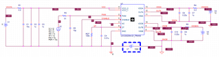
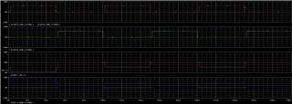
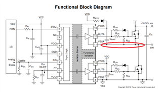
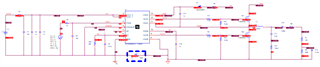
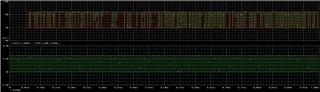
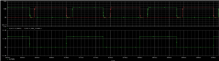
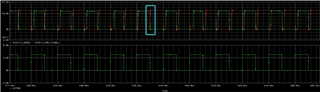
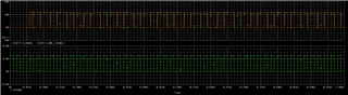
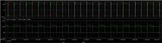
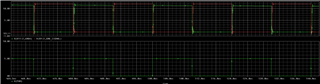
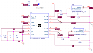
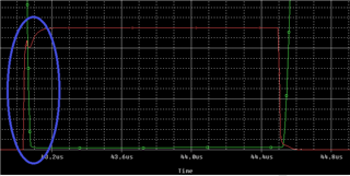
We are trying to run Spice simulations using the PSpice for TI tool in order to analyze the UCC20225A behavior. Nevertheless, it seems that the Dead Time (DT) implemented in the model is not working, as the two output signals (OUTA and OUTB) are overlapped, regardless of the resistor value connected on the DT pin. Please, find attached two images. Thank you in advance.

Best regards,

  • Hello,

    Thanks for reaching out.

    We're reviewing the details of the problem and will get back to you promptly.

    THanks.

    -Mamadou  

  • Hi Mamadou,

    I will wait for your reply.

    Thanks,

    Best regards,

  • Hi Zhonghui, 

    I was able to confirm that the PSpice model is working as expected based on the following simulations. 

    As you can observe in both simulation the delay time for the model is working as expected. 

    Would you be able to share the deign files with us? I would recommend beginning with the set up simulation we have in the ti.com page for the device. 

    Let me know if this helps and thank you very much for reaching out. 

    Sincerely, 

    Francisco Lauzurique 

  • Hi,

    Thank you for your reply.

    I have been able to perform the simulation you propose and the result is correct. However, I am trying to simulate a circuit from the datasheet (attached image), and I cannot get the simulation right.
    The problem I see is that when VSSA is connected as in the attached image, that is, when VSSA is not connected to VSSB. In this case, the Dead Time is not generated well.

     picture.docx

    Thank you.

  • Hi Zhonghui, 

    Thank you very much for reaching out. I need more information about your issues to understand what is happening. 

    Can you provide more information here: 

    1- Can you share your design  files?

    2- Would you be able to show waveforms for the issue you see? Include inputs and outputs waveforms 

    Best, 

    Francisco Lauzurique 

  • Hi Francisco,

    sorry for the delay!
    Please find attached .zip with all the required information.

    TIsupport.zip

    Thanks a lot.

    Best regards,

  • Thanks Zhonghui,

    My colleague Francisco is reviewing your latest files and will get back to you promptly.

    Regards,

    -Mamadou 

  • Hi,

    thanks.I will wait for your reply.

    Best regards,

  • Hi Zhonghui, 

    Thank you very much for your patience here. I was unable for some reason to open your PSpice simulation files. However, I try to create something similar to what you mentioned during your question. I still see the dead functioning as expected when switching a half bridge architecture. 


    Please let me know if this is something similar to what you currently have in your design file. 

    UCC20225A-Q1_PSPICE_TRANS.zip

    Let me know if this helps to prove the idea for the correct behavior of the DT pin. 

    Sincerely, 

    Francisco Lauzurique

  • Hi,

    Please find attached an image with the circuit from the datasheet which I want to reproduce. I have marked in red the main differences with your example. VSSA is not connected to GNDA as in your example, but is connected to the wire between MOSFET transistors.


    Thank you.

    Regards,

  • Hi Zhonghui Xu, 

    Let me go ahead and check this new set up you have proposed. I will have a final answer here by Monday. It could be that our model is not working properly, and if that is the case I will request for an update on the model. But let me first try to do your recommended set up. 

    Sincerely, 

    Francisco Lauzurique 

  • Hi Zhonghui, 

    I was able to create the correct simulations based on the feedback you provided me.

    The following waveform shows the transient simulation until the output becomes stable and the voltage are well defined. 

    The following image shows the expected DT behavior 

    The following image shows a case in which the DT pin fails as you were suggesting 

    Is this agreeing with what you see in your simulations? Do you see random failures as shown here or do you observe consecutive failures? 

    I am going to reach internally to the Pspice model designer to request for this issue to be fixed for the next generation of devices. 

    However, I was able to fix the issue by decreasing the PWM and decreasing the pulldown resistance to have a higher pull down. 

    In this case the DT pin was behaving as expected during simulations. The two waveforms bellow show how the outputs will not be overlapping any further 

    Summary: 

    - I am not sure of the parameters for the GaN you are using, but you should ensure that the driver can correctly switch the GaN fets at the expected frequencies. Notice that for my simulations I used different GaN devices, and by decreasing the the switching frequency I was able to obtain the correct behavior. I would recommend trying a similar approach here.

    - I also noticed that your bootstrap circuit is a bit low on capacitor values based on the design parameter values you have. I recommend taking a double check on the design of this part of the circuit before creating a final design. 

    Thank you very much for reaching out. I hope this detailed explanation helps and feel free to reach out for more questions. 

    Sincerely, 

    Francisco Lauzurique