This thread has been locked.

If you have a related question, please click the "Ask a related question" button in the top right corner. The newly created question will be automatically linked to this question.

LP38512-ADJ: No output voltage issue after many times powering on and off

Part Number: LP38512-ADJ
Other Parts Discussed in Thread: LP38512,

Hi Team,

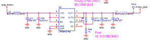
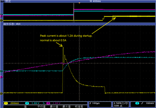
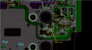
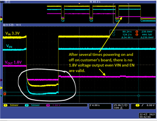
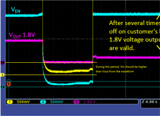
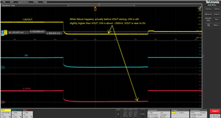
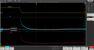
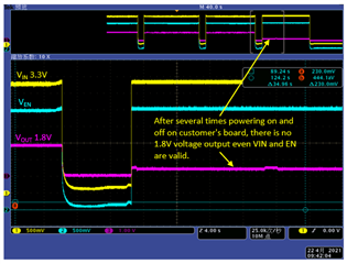
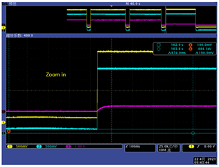
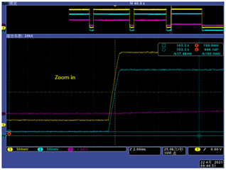
Our customer is using LP38512-ADJ for 3.3V to 1.8V application for DLP DMD power supply, but recently they found there is about 1 in 10000 probability for LP38512 no 1.8V output issue after many times powering on and off. We captured some waveform as below, can you help to analysis what's the possible cause for this behavior?

Thanks.

  • Hi Jacky,

    I'm reviewing your question.  Please provide 3 business days for a reply.

    Thanks,

    - Stephen

  • Hi Jacky,

    If you could provide a schematic of the LDO circuitry I could review it for any issues.

    Does this behavior happen on more than one LP38512?  I know this is a time consuming test but would it be possible for the customer to do an ABA swap, where they take another LP38512 and swap them then rerun the test to see if the issue comes back? 

    I will be heading into the lab today and can check our inventory incase we need to do any testing here, although the EVM will have to be built.

    Thanks,

    - Stephen

  • Hi Stephen,

    Attached is customer's schematic for this device. We did the A-B-A test, and this issue was followed by the failure device. But if we put the failure device to a standalone board to check again, we will never reproduce this issue. The failure rate for this issue is about 1/10000 on customer's production line. So far we can only capture the failure on customer's product with above waveform, but we do not know why it failed.

    Thanks.

  • Thanks Jacky, I just received your latest update and I'll look at this further tomorrow AM.  I reviewed our stock of components and unfortunately we do not have any spare IC's to populate onto a blank EVM.  I do have the blank EVM and I will order some spares incase they are needed for this effort, which should take 5 business days to arrive.

    I'll provide additional feedback tomorrow.

    Thanks,

    - Stephen

  • Hi Jacky,

    The schematic looks fine.  Can you tell me more about the customers application?  What is the load current during these tests?  Are these measurements being made right at the LDO or further away on the CCA? 

    Perhaps there is noise in the system which is affecting the LDO?  I don't have any data suggesting this device is noise sensitive, but it might be good to narrow this out.  While it is obvious from the screen shots that conducted noise does not exist, perhaps electric field coupling or radiated noise exists in the system.  Can you confirm that a ground plane exists below the LDO?  Can you confirm that radiated noise is not present nearby?

    I've requested samples of this component incase we need testing at my lab.  The usual shipping time is 5 business days.

    Thanks,

    - Stephen

  • Hi Stephen,

    The load current normal is about 0.5A, peak is about 1.2A during startup as below capture. And I don't think it related to OCP or OTP protection as the failure device is latched without recovery.

    Regarding to the noise issue, as you can see from the waveform we captured, we do not find any obvious spikes or other things on the LDO input and EN pins. We will send you customer's PCB layout for this circuit for your review when we get it.

    Thanks for the support.

  • Hi Stephen,

    Please refer to below customer's PCB layout, it looks good from my side for LP38512 based on my experience, and it is a 6-layers board. Please help to check from your side, and I don't think it is related to layout and noise issue.

    For what I'm suspecting is only the floating voltage about 190mV as we captured above when powering off, but I do not know how it influenced to this device's behavior without normal output.

    Thanks.

  • Hi Jacky,

    Those values of current look fine to me.  However, could the device be entering thermal shutdown?  At 0.5A load and (3.3Vin - 1.8Vout) of headroom, the part will dissipate 0.75W.  With a JEDEC standard 168 C/W thermal resistance for this package, the junction will heat up 126C above ambient.  I would confirm that the temperature is not an issue here, can the customer measure the temperature of the device?

    Thanks,

    - Stephen

  • Hi Stephen,

    We confirmed that it should not be a thermal issue, as you can see the startup waveform, this issue only happened during powering on and off, at this moment, the load is not drawing much current and the IC has no obvious thermal heating up. Also, if it is a thermal issue, the no output issue should not exist as always, as thermal protection is not latched.

    Thanks.

  • Hi Jacky,

    I missed the part where you mentioned this is latched.  How does the device recover, or once it latches does it never recover (even if you turn off all power and come back some time later to test again?)

    Let me review this again in the morning, however we may need to recommend the customer return this unit for FA if nothing else comes to mind.

    Thanks,

    - Stephen

  • Hi Stephen,

    When there is no output, you can only recover it by powering off and powering on again. Once there is no output, it can not be recovered by itself anymore even VIN and EN keeps normal.

    Thanks.

  • Hi Jacky,

    I've noticed that Vin drops below Vout during these tests which can cause reverse current flow.  Can the customer please eliminate this reverse current flow to see if the issue goes away?  One common method is to add a low voltage schottky diode from Vout to Vin to reroute this current around the LDO.

    Thanks,

    - Stephen

  • Hi Stephen,

    Sorry for that I can not understand what you mentioned for Vin drops below Vout for these tests, what we observed for the failure is Vin is always above Vout, please refer to the first post pictures.

    Thanks.

  • Hey Jacky,

    Right in this location Vin < Vout which can cause the reverse current flow issue.

    Thanks,

    - Stephen

  • Hi Stephen,

    From the zoom in waveform, I don't think there is Vin<Vout happened. I will ask customer to capture the detailed waveform again and feedback to you.

    Thanks.

  • Hi Stephen,

    Please refer to below customer's new capture, actually before VOUT startup failure, the VIN is still higher than VOUT which is near to 0V. So we don't think it is related to reverse current flowing from VOUT to VIN.

  • Hey Jacky,

    It still looks like reverse current can be happening during the falling edge of the waveform when the device is turning off.  Can the customer zoom in to see the falling edges better?

    Thanks,

    - Stephen

  • Hi Stephen,

    Please refer to below capture for what you mentioned, please help to check if there is any issues. Thanks.

  • Hi Jacky,

    I am reviewing this and will reply soon.

    Thanks,

    - Stephen

  • Hi Jacky,

    Please have the customer initiate the return process.  There is a page on TI.com which gives guidance on this if the customer has not done this before.

    https://www.ti.com/support-quality/additional-information/customer-returns.html

    Thanks,

    - Stephen

  • Hi Stephen,

    Do you mean we need to put this device for failure analysis process to CQE team? I'm having concern that this may not be IC failure as if we put this device on standalone board out of customer's system, we can not reproduce this phenomenon. This issue only happened in customer's system but we can not locate the root cause.

    Thanks.

  • Hi Jacky,

    My thought is to start the return process to have us review it as an FA.  The device is not behaving as it should even with normal waveforms on Vin and Vout. 

    One last test would be to compare known good waveforms to these waveforms you have provided.  But I don't think they will look significantly different, except the failure itself will not be repeated on a known good unit.

    The customer could also send us the failing unit on their hardware, and we could conduct the same tests here to observe the failure.  Is that something the customer would prefer?

    - Stephen

  • Hi Stephen,

    Customer prefers to return the failure device to us only as if we replaced the failure device by another one in the system, issue will be closed as well. Another limitation is this device is used in their Laser TV DLP DMD board, and the whole machine is too large and can not be shipped out from their side. Customer has agreed to return the failure for FA process and will let you know when submitted the FA request.

    Thanks for the support.

  • Thanks for the update Jacky.  We'll watch for the FA return on our end.  I'll close this E2E ticket but if you need additional support please let me know.

    Thanks,

    - Stephen