


Other Parts Discussed in Thread: LM5175
G'day,
I'm using an LM5176PWPT to provide a 12V rail for my device from a 7-27V input. I've read through the datasheet a number of times, and have used the Webench tool to construct a suitable schematic. I've followed the layout guidelines presented in the datasheet, which has resulted in the below rough draft:
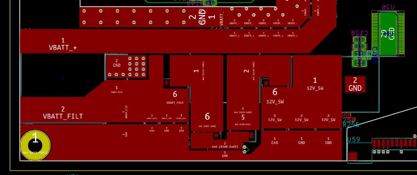
Without the top layer fill so you can see the individual components:

A couple of notes:
- The outside yellow line is the edge cut of the PCB
- The outside white border is the 2mm keep out
- This is a 4 layer board (signal, GND, PWR, signal); red is top signal, green is bottom signal, pink is PWR.
- U26 is the LM5176, shown on the reverse side of the board (top right corner); I obviously haven't yet routed anything to/from it.
The datasheet shows the LM5176 being placed on a large ground fill. As my power circuitry is at the bottom of my board, I'm somewhat pressed for space, so can't have the LM5176 on the same/top side of the board as the datasheet suggests. My question is as follows: if I use a ground fill on the reverse side of the board, and make the required connections to the top ground fill as well as the solid GND plane (layer 2) with vias, can I place the LM5176 on the reverse side of the board, directly underneath the MOSFETs, inductors, etc.?


