This thread has been locked.

If you have a related question, please click the "Ask a related question" button in the top right corner. The newly created question will be automatically linked to this question.

LMS3655: Top an bottom copper weight

Part Number: LMS3655
Other Parts Discussed in Thread: UCC27511,

Hello everyone,

I am using the LMS3655AMRNLT synchronous Buck converter to step down 24 V to 12 V. The schematic and PCB design are almost done. The last one was made following the indicated recomendations of it datasheet (http://www.ti.com/lit/ds/symlink/lms3655-q1.pdf ). On page 42 it is said (see highlited text):

As i get it, It seems that those layers require that amount of copper so that the heat dissipation could be possible. My question is: what if i use 1-oz copper top and bottom layer instead of 2-oz, but I make up for with a heat sink placed right behind the chip -see the arrow of the right image- (of course, following the other recomendations, specially the "huge" top and bottom ground polygon)? would the convert work properly?

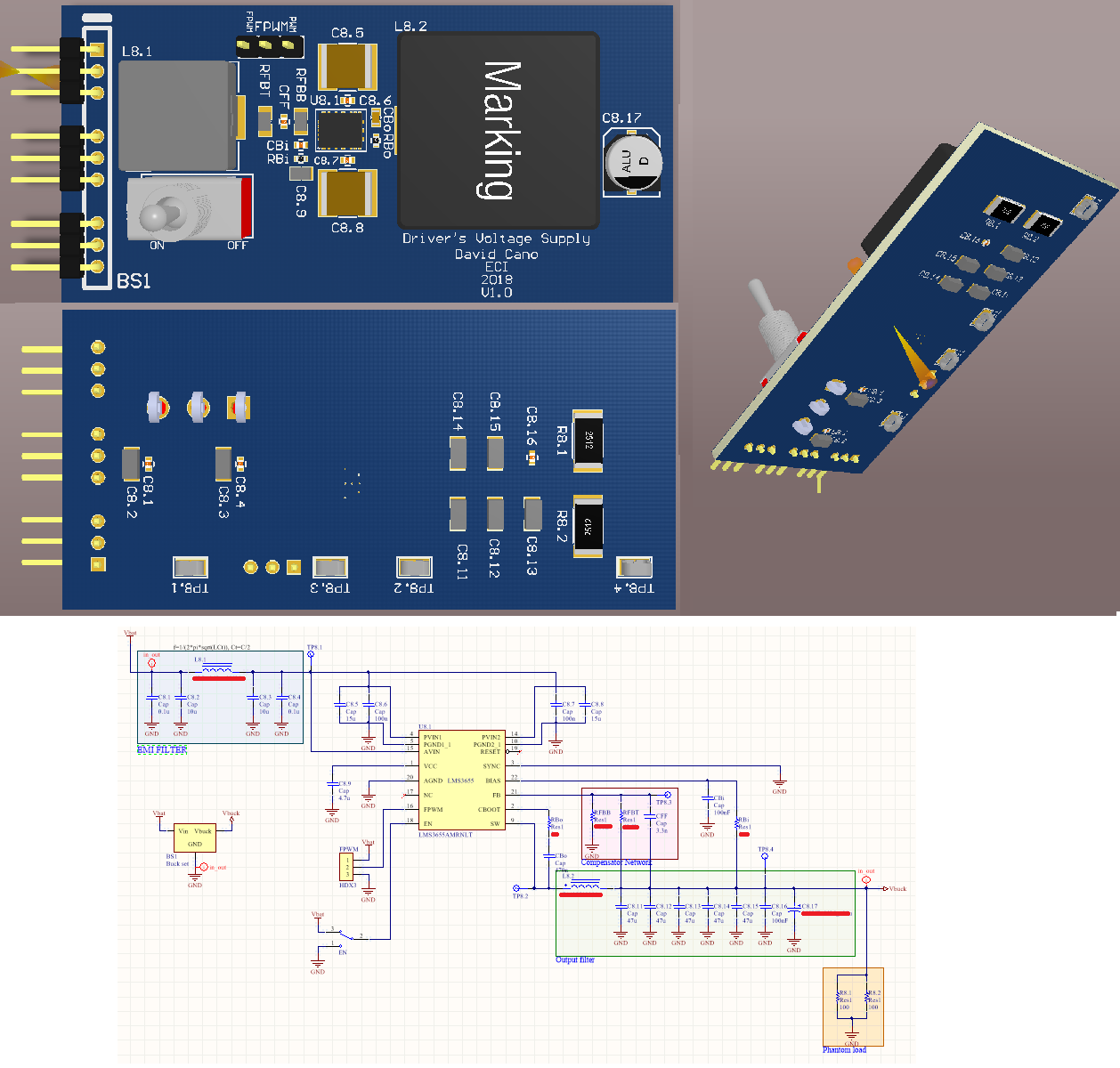
FInally, I want to add that the size of that module is about 75mm x 35 mm.

TI team or reader, as always, thank you for your help.

Any further comments would be appreciated.

Best regards,

David Cano.

  • (of course I would use a good via stitching between ground polygons located in every layer)
  • David,

    Thermal questions are difficult to answer with certainty. 1oz over 2oz will be warmer, especially at 12VOUT (presuming close to 5.5AOUT). The back-side of the board will be warm and the heatsink will help but the specifics will depend on the size and shape of the heatsink as well as how much area connects the heatsink to the board. If 1oz vs 2oz was a cost saving consideration then the cost of a heatsink to achieve the same performance may not be possible or worth the trouble.

    But, as I said, I can't say with certainty what will be the better option. The best way to know would be to build the board and test it.

    -Sam
  • Sam,

    Thank you for your answer. You did totally get the real reason of my question: cost. Would it help if I tell you that the converter is going to feed the current mode controller (of a push-pull topology operating at 100 kHz) that sources 500 mA per stage (UCC3808). Every single output of it would be the input of a GaNFET driver (UCC27511) which is capable of sourcing a peak current of 4 A. What I am trying to tell you here is that is going to be a high peak current, but once the Ciss of the GaNFET (EPC2032, QT=15nC) has reached its "nominal charge", the current would not be that high as the peak one.

    I am looking forward to your answer.

    Regards,

    David.

  • David,

    So as I understand:
    LMS3655 outputs 12V at 4A peak (every time the GaN driver switches high at 100kHz) and 500mA when the driver does not switch. That would bring down the average current quite a bit. I think this should be fine. The only way to know for sure would be to build it and test it.

    -Sam