This thread has been locked.

If you have a related question, please click the "Ask a related question" button in the top right corner. The newly created question will be automatically linked to this question.

TPS54560B-Q1: Fsw and compensation components values in buck and inverting applications?

Part Number: TPS54560B-Q1
Other Parts Discussed in Thread: TPS54360B, TPS54560B

Hello to all,

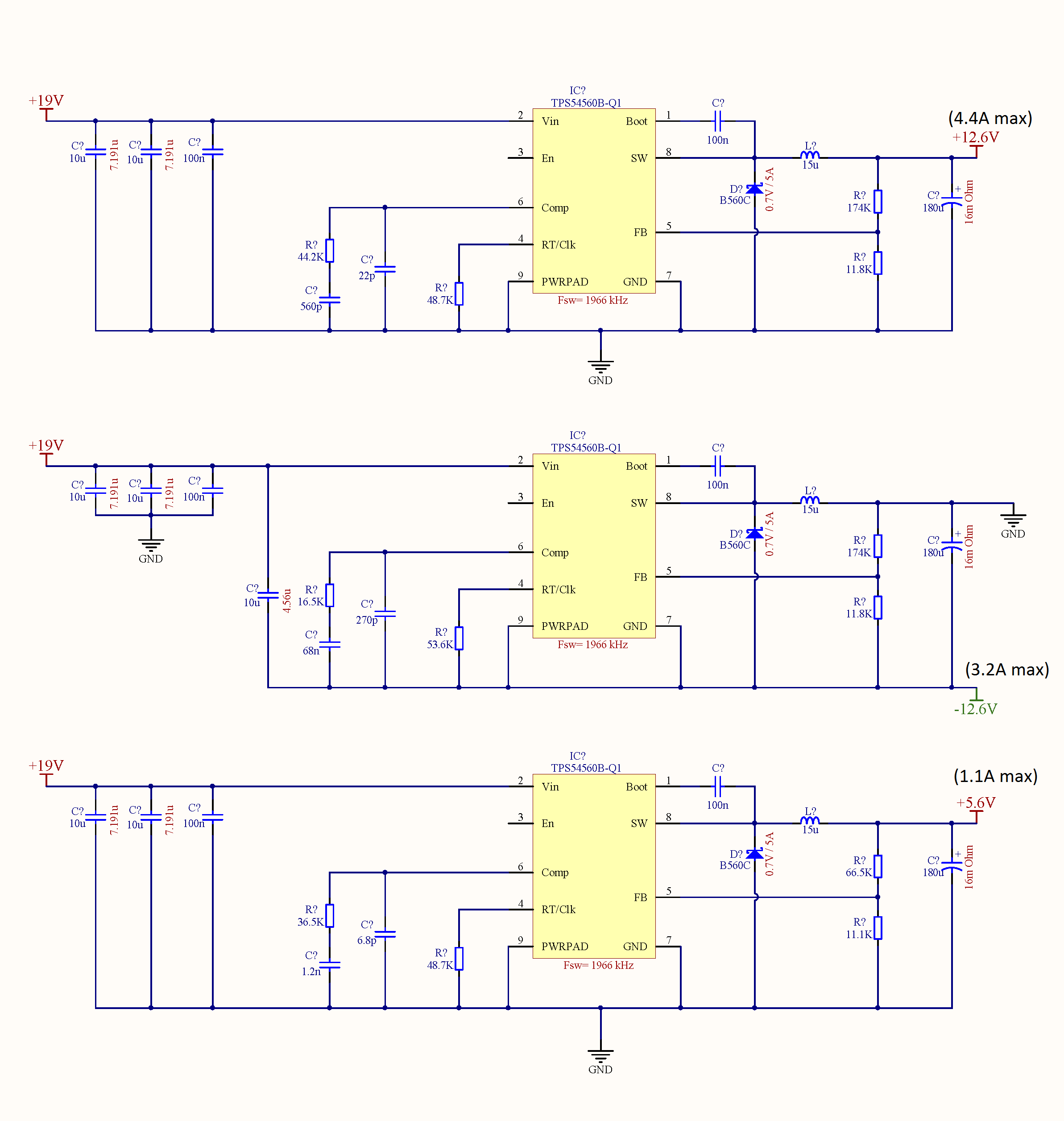
Here is my PSU schematic. You can see the derated cap values in red text strings. I've used TPS54560B and TPS54360B in this design and also used Webench Tool for both my +12.6V and +5.6V rails. Hence Webench does not support the inverting application, i've followed SLVA317B and Excel sheet. But i have a few questions;

1) Both my +/-12.6V rails using TPS54560B but frequency resistor values are different for the same Fsw (1966 kHz). Is it OK?

2) Do input and output capacitor values look normal? Actually they are way above than minumum value which is 3uF according to datasheet but there is no info about upper limit :) I need get rid of the ripple and nois as much as possible. That's why i'll use linear regulators after this.

3) Compensation values are different for buck and inverting rail. I've calculated over and over again. Found the exact same values with Excel sheet. I assume they are ok but found some schmatics online that shows some people uses the same components for both buck and inverting application.

4) If is there anything you see on the schmatic is needs to be fixed or if you want to give me some tips it will be awasome:)

Thank you in advance

  • Hi,

    1) I think the frequency resistor should be the same regardless if you use the IC as a buck or inverting buck. Therefore if you want to set the same switching frequency, therefore you should use the same resistor. 

    2) Yes, the input capacitor looks ok to me

    3) This one the compensation value should be similar. You can think of it as an upside down buck. I would try using the same compensation between the buck and inverting buck as my first try.

    One of the difference on the inverting buck boost topology is the introduction of right hand plane zero (Fz2 on the app note). Therefore you want to have your crossover frequency of the loop before this right hand plane zero. The location of this right hand plane zero is dependent on your duty cycle and value of inductor with the emphasis on inductor. The larger the inductor, the lower the location of this right plane zero.

    You can see the calculation on the app note that you mentioned and figure out the location of this right hand plane zero. 

    If your crossover frequency is lower than the location of this right plane zero then in general you should be ok. 

    4) It seems to me that your schematic looks ok. One thing that i would be concern about is the thermal when you run at this high frequency of 1966kHz. You can also try to check your design on evaluation module and make sure the thermal is ok when running at this high frequency.

    Thanks

    -Arief

  • Ok so i will use the same components i've used in buck config for the inverting config.

    This is a direct quote from SLVA317B ''The crossover of the power supply should be set between the ƒp1 and 1/3 of ƒz2 frequencies.'' My ƒp1 314.5 Hz,  ƒz2=35059 Hz and ƒco=3318 Hz. So it should be OK.

    I'm also worried about the thermal performance. I'm plannig to use heat sinks but have not found any yet. If you can help me with that it would be great :) Or i may use fans.

  • Hi,

    In case of thermals, i would reduce the switching frequency if possible just to increase the efficiency. 

    Therefore you have less power loss and the components will be cooler just by properly using the DAP underneath the IC attached to the board as heat sink

    Thanks

    -Arief

  • Thank you again for the answer,

    I've reduced the output current so now i need 2.3A on 12.6V rail and 1.6A on 12.6V rail. That's why i've switched to TPS54360B but still have problems with the determining component values.

    Of course first i've used Webench Tool and realise compensation components and switching frequency resistor values are different from my calculations and Excel Calculator Tool. I mean they are vastly different not even close. My calculations (according to formulas on datasheet) match with the Excel Sheet. 

    Here is Webench Circuit. Here are the changes that i want to do;

    Increase input cap to 2x10uF ( 16,25uF derated) (Total ESR= 1 mili Ohm)

    Increase inductor to 3,3uH (DCR= 8,6 mili Ohm)

    Increase out cap to 6x10uF (ceramic) ( 51,7uF derated) ( Total ESR= 0,8 mili Ohm)

    1)Should i change the compensation values as well? And if i should, how can i calculate them? Again Webench calculations and Excel calculations do not match.

    2)And of course Fsw. I need to know resistor value for 2.5MHz

    Thank you advance and please keep in mind that i will use the same circuit in Inverting Topology.

  • Hi,

    I believe we cover this on the other thread. For now i will close this thread and continue the discussion on the other one

    Thanks

    -Arief