This thread has been locked.

If you have a related question, please click the "Ask a related question" button in the top right corner. The newly created question will be automatically linked to this question.

UCC28600: UCC28600 increases output voltage when the input voltage becomes low

Part Number: UCC28600

It would seem normal that the output cannot be maintained when the input voltage drops. However I have the problem that the controller keeps switching and actually increases the output voltage uncontrollably.

The power supply is designed for an input voltage of 320-780VDC and an output of 48V 40W.

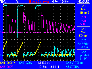
The issue occurs when the input voltage drops underneath 150V and with no load on the output. The compensation network pulls the FB pin to approximately 0.1V. the aux supply voltage rises from 15V to 20V at this point, but the gate voltage drops to about 5V. It keeps switching and the mosfet becomes incredibly hot within seconds.

I am at a loss here, it would seem that something is wrong with the controlchip (as it keeps switching with 0v feedback and gate voltage does not match the supply voltage) But I have the same problem after replacing the chip.

At 350V it works perfectly.

Could this be an EMI problem?

  • At this low voltage the freewheel voltage (the sine after the reflected period) goes below 0 and induces a negative current through RCS. This might have something to do with the issue.

  • Hello Daniel,

    Thank you for your interest in the UCC28600 flyback controller. 

    I do not believe that the problems you are encountering are due to EMI.  The information in your last post is a good clue, since negative current in Rcs implies a negative voltage at the CS input.  The absolute maximum rating for negative V on CS is -0.3V.  In general, excess voltage below GND on any pin may result in substrate injection of high currents into normally back-biased junctions and can turn on unwanted parasitic transistors. If this happens, it is unknown how the IC will respond since the normal circuits are disrupted.    

    Since the negative current in Rcs increases as your input voltage goes down, the resulting negative voltage on CS also increases.  To prevent excess neg-V on CS, I recommend to add a 1A schottky diode from CS to GND, such as 1N5817 or equivalent.   I prefer this part over others because it has a very low forward drop compared to that of small-signal schottkies for a given current.  Connect anode to GND, cathode to CS, and Rpl will limit the forward current.

    There may be other causes of your converter's problem behavior, but adding the schottky diode is to solve certainly worth doing as a test to see if it solves the problem.  If you expect that input voltage will routinely or even occasionally drop to 150 V or lower with the converter still running, then it is certainly a necessary precaution to add one simply to prevent any possibility of problems from the CS input, even if there are other causes.

    Another possible cause or problems is if you have more than 390pF from FB to GND.  Excess time delay on the FB signal can confuse internal circuits trying to determine which mode to operate in based on timing.  Poor coupling between the Auxiliary winding and the Secondary winding may also lead to timing issues at the OVP input.  FOr the 5-V gate voltage symptom: is this voltage at the MOSFET gate to source, or at the OUT pin to GND?  Is there a series resistor between OUT and the MOSFET gate?

    Can you provide waveforms of the burst during this condition, showing drain voltage (50V/div), OUT voltage, CS voltage, and OVP voltage at different sweep rates?  One slow enough to capture 2 or 3 bursts, one fast enough to capture all of 1 burst, and one fast enough to capture 1 or 2 cycles within a burst, please.

    At this time, excess negative voltage at CS is the prime suspect and a good schottky diode show fix it. 
    In order to ascertain any other possibilities it would be very helpful if you can provide a schematic diagram of your converter using the UCC28600, and the waveforms.  Also a copy of your Design Calculator would be helpful, if you used one for design. 

    Regards,
    Ulrich

  • Hi Ulrich,

    Thank you for your elaborate reply!

    Here are the schematic and calculation xls:

    UCC28600 huplvoeding 320-760VDC 40W.xls

    I tried a 30V schottky (bat54s) across the CS pin, this did nothing whatsoever. I will order a lower voltage schottky to try next. the signal on the CS pin however never goes below 100mV when I check it with a scope.

    I managed to capture some events where the problem starts. At a lower input voltage the device sometimes switches at the wrong moment (not at the valley). The next period it looks almost like the gate output is floating. Then it starts to oscillate.


    Ch1: Current sens across resistor R23/24, Ch2: OUT (pin5 of U1), Ch3: VDS of Q1.

    I noticed that the voltage at the out pin also went a bit below 0V, so I added a schottky diode between gnd and the out pin. This stopped the oscillation (and the output rising uncontrollably), but did not fix the problem.

    After adding the diode I took some more shots with the OVP pin at CH4:

    At a higher input voltage it always switches in the valley and this effect is not present.

  • Hello Daniel,

    Thank you for all of the additional information.  Since the CS input is not going significantly below GND, adding the schottky diode there will not change anything, I agree.

    Your observation of OUT going below GND is significant.  Unfortunately the datasheet does not specify this pin very well, so I don't know what the limitations are.  This device was designed around 2005 and the original designers are no longer with TI, so we'll have to deal with the symptoms as we see them.  Adding the schottky to OUT did improve the operation, so that is the direction to follow. The BAT45S is a small-signal diode and cannot maintain a low Vf at higher currents. 

    I looked up the 2SK4177 MOSFET and it has unusually high Crss (Cgd) compared to the typical 600~650V FETs that I am used to working with.  I think this may have a bearing on the situation.
    Your design has a reflected voltage of ~350V.  At 150Vdc input, the stored energy in the switched-node capacitance tries to drive the drain voltage to -200V below GND, but of course the body-diode prevents that.   But the high Crss may be pulling significant current out of the OUT pin, which pulls that pin below GND, too.  Your signal-diode schottky clamp is helping by reducing the Vneg.

    I suggest to (a) use a stronger schottky clamp on OUT, and (b) increase your gate resistance R4 from 15ohm to 47~50ohm. 
    This will reduce the current during this situation.  It will also reduce it during normal operating conditions, so a bypass diode across R4 will be needed to aid turn off.  High turn-on drive is not important because there is no primary current (except capacitive discharge) in the primary at turn-on.  You just need high current drive at turn-off and the bypass diode across R4 will allow that.

    I believe that the delayed non-valley switching is not an issue with respect to the Vneg.  It may increase switching loss at very low input voltages.  As I understand it, valley-switching is accomplished by sensing the Vaux zero-crossing at the OVP pin and adding a time delay before driving the OUT signal.  The time delay was determined using typical off-line MOSFETs circa 2005, when Coss was not as highly non-linear as it is now.  The Vneg at OUT may be influencing the valley-detecting timing circuit somewhat.

    You last 2 screenshots of OVP signals still show that the OUT voltage rises to ~5V during the resonant ringing.  These partial turn-ons are injecting enough energy to keep the ringing from damping out.  I am hoping the increased R4 and stronger OUT clamp diode will eliminate this symptom.  In other words, I hope that the ~5V drive will no longer be there and the ringing should damp out between bursts.  Please try my suggestions above and let me know what happens.

    Regards,
    Ulrich

  • Hello Ulrich,

    The schottky diode I added on the out pin was a 3A type. I added the 47Ohm gate resistor and a bypass schottky towards the out pin for a fast turnoff. The ringing on the gate was still there.

    Following your remark on the High Crss got me thinking. I went back to the original situation (no schottky and 15Ohm gate resistor) and added a 2.2nF capacitor on the gate pin of the mosfet to improve the ratio Cgs to Cdg (make the gate capacitance leading). This gave a similar result. some ringing remained present on the gate but no unwanted turn-on. I used a different voltage scale for the gate voltage at CH2.

    The next thing I noticed is that this effect always happens at the end of a burst period. Every single one, even at higher input voltages. There is some delay after the last pulse before the gate starts ringing. It almost seems that the IC goes to a low power mode after a burst and reduces the drive current of the out pin.

    To keep the gate voltage low I tried a millerclamp circuit to the gate. The current required to pull the gate down is much less this way. This kept the gate voltage low enough for me to feel comfortable with this solution. 


    An alternative solution would be to use a different high voltage mosfet, like the C2M1000170J. It has a much better ratio between Qgd and Qgs. Downside is that it has a lower gate threshold voltage. I think I will try this one next.

    Thank you very much for your time and assistance! It is very much appreciated!

    Kind regards, Daniel Eindhoven