This thread has been locked.

If you have a related question, please click the "Ask a related question" button in the top right corner. The newly created question will be automatically linked to this question.

UCC2897A: UCC2897A Hardware Dbugging Problem

Part Number: UCC2897A
Other Parts Discussed in Thread: , TLV431B

UCC2897A POWER SCH.pdfHi TI

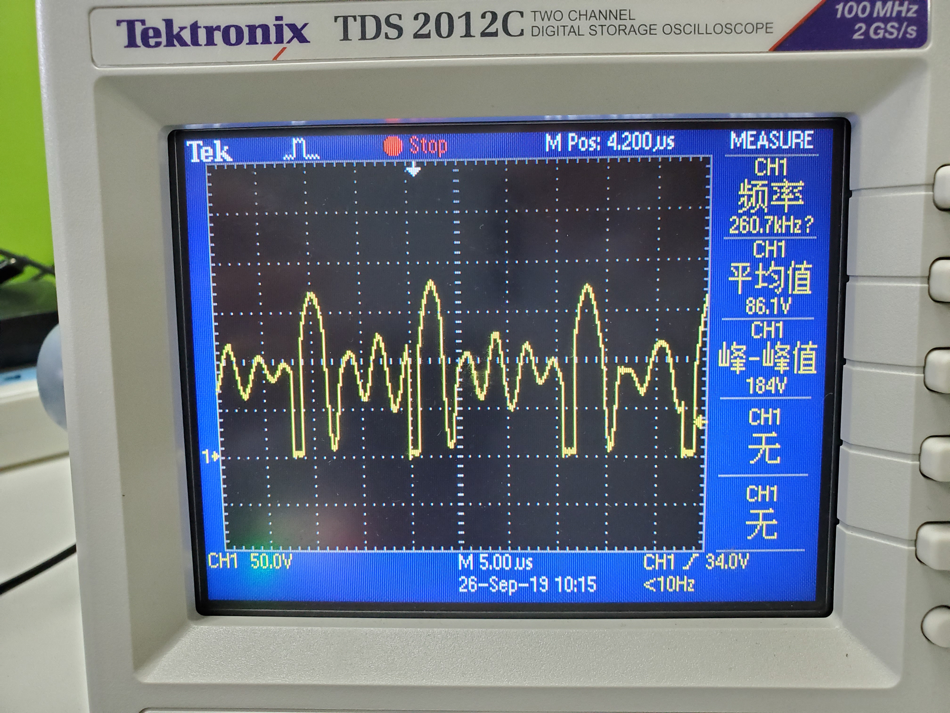
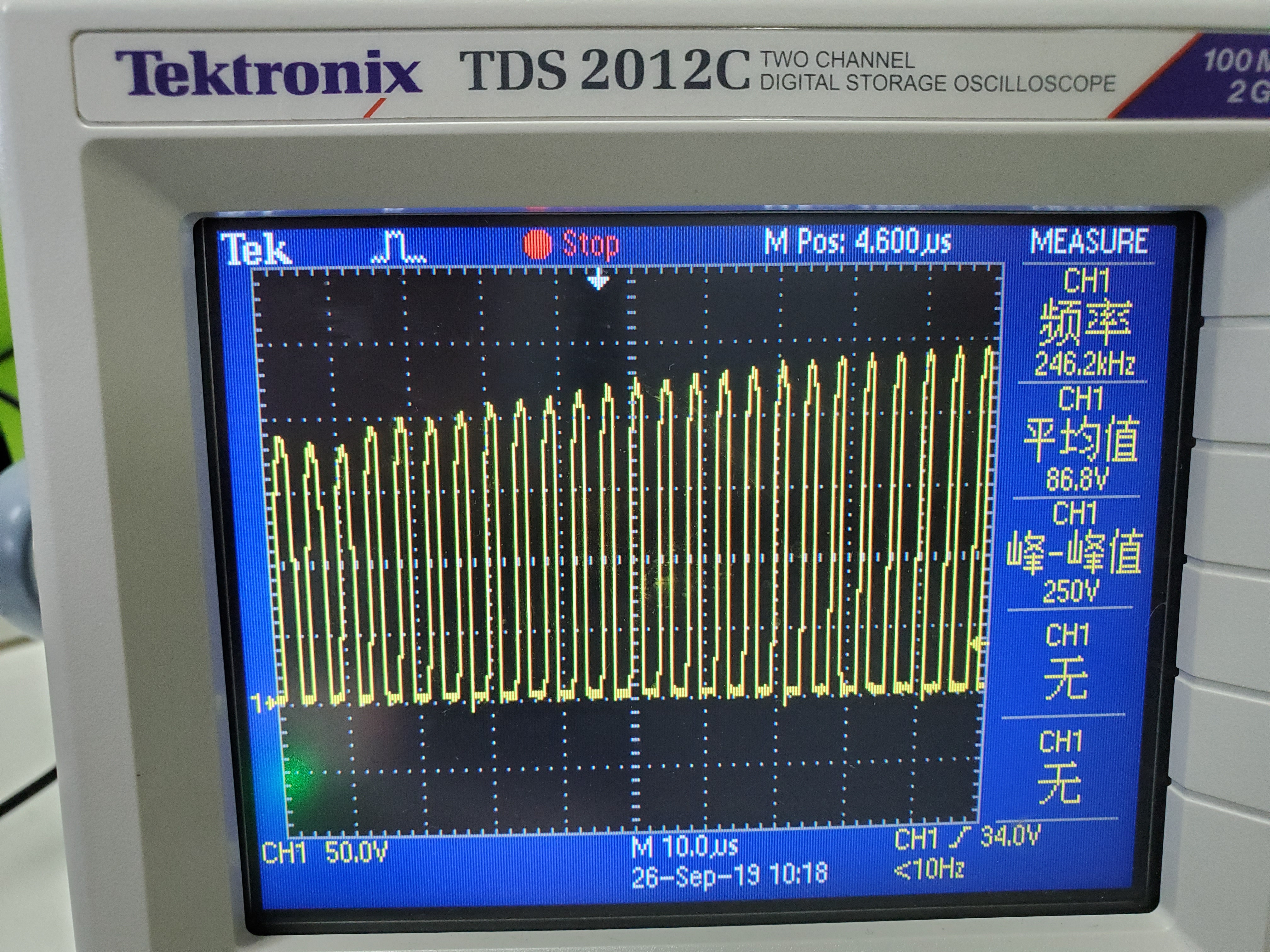
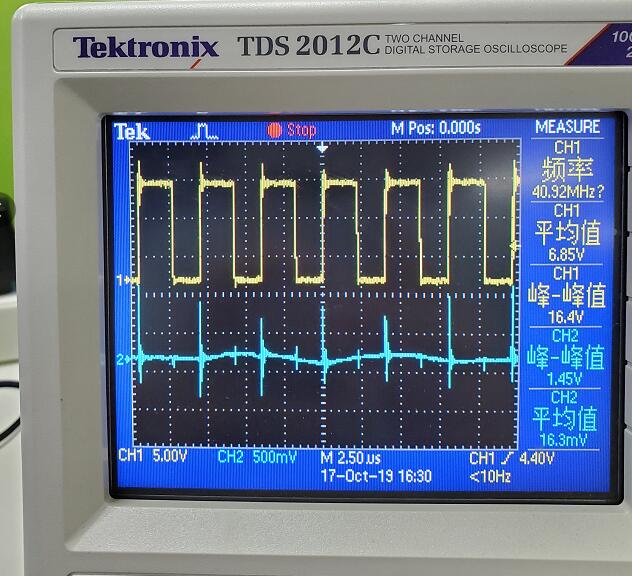
I recently had a project that used active clamp forward excitation topology with 66-160vdc input and 48v@3A output.The schematic diagram is attached.Currently it can output 48V, but not with load.FB is about 2.1v when no load, and 5V when light load, and the output voltage will be slightly reduced, increase the load voltage drop more severe, FB is still 5V.
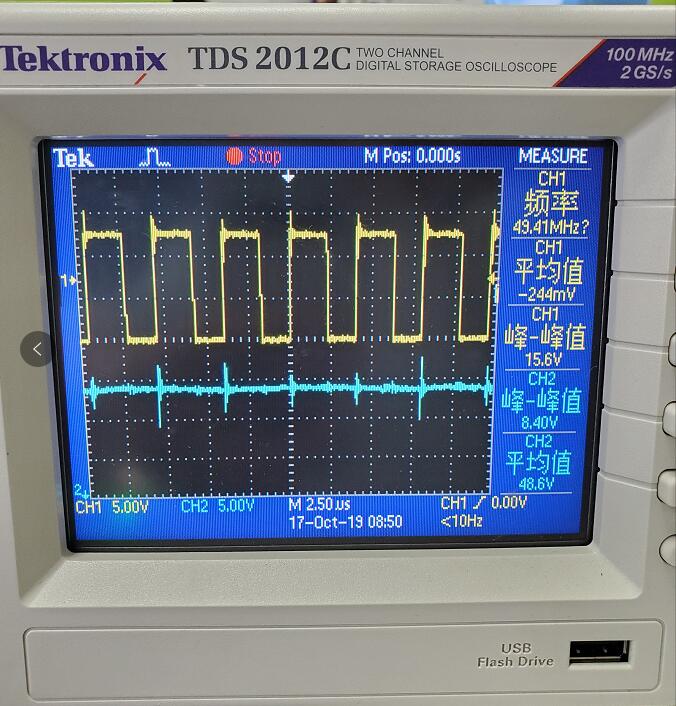
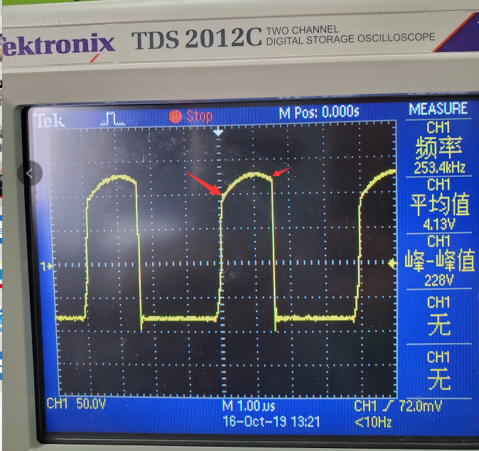
When I adjust the feedback circuit, FB is about 3V when there is no load, and the voltage will rise to about 100V when the power is on.I want you to help me analyze the reason. Personally, I think the parameters of the feedback circuit are not set well.But I tried for a long time and still no result.
In addition, I want to know the Compensating the Feedback Loop parameters how to calculate?

  • Hi Tracy, an expert will get back to you soon.——Teng

  • OK,Looking forward to your reply!

  • Hi Tracy,

    Firstly, you have to correctly biased the TL431B , TL431B require a minimum cathode current for regulation, it is 0.7mA. So please parallel a 1K resistor on the opto-coupler diode. I don't know how you adjust the loop compensation that let you output voltage up to 100V but the FB voltage is still 3V.

    One thought from my side is. since your BIAS2 voltage is around 9V.  the minimum cathode voltage of 431 is 2.5V , plus opto-coupler diode forward voltage ~1.2V.

    we can get the Ib current through optocoupler is around 2.4mA , look to primary side , R31= 1k , If you want to pull FB voltage down to 0V in no load condition.

    The CTR of opto-coupler should be >208% , I am not sure if all of components value demonstrated in the schematic are the same with your debug.

    In other words , you can try to increase R31 from 1K to 2K , or decrease R28 from 2.2K to 1K .

    The third , what's the purpose of C20 which parallel on cathode and anode of 431 ? can you try to remove it . as well as C19 ?

    Attached a application notes for your reference , you can find the guideline of how to design loop compensation in it .

    Thanks.

    4863.Understanding and Designing an Active Clamp Current.pdf

  • Hi Jaden,
    Thank you for your reply.According to your suggestion, I parallel the 1K resistor in the optocoupler diode and adjust the feedback resistor. Currently FB is in much better condition than before.But many reference designs do not do this, such as UCC2897AEVM.

  • Hi Tracy,

    That is because the 431 chosen on the ucc2897A EVM board is TLV431B which minimum cathode current requirement is only 55~80uA.

    Far less than TL431B required minimum cathode current. This minimum current can be provided through optocoupler diode even in heavy load condition.

    Hope can answer your question.

    Thanks.

  • Hi,Jaden

    Thank you for taking the trouble to help me out.

    When I used the oscilloscope to measure the waveform, I found that the Vds waveform of the main switch tube was a little abnormal.The waveform is shown in the attachment.
    1. In the absence of load, the waveform is irregular;
    2. In the case of light load, the Vds waveform is shown in the figure, accompanied by a slight inductive noise;
    3. Continue to increase the output power, the waveform is no longer equivalent, the inductive noise is louder, continue to increase the load, MOS burn out.
    I guess it is caused by insufficient clamping of C4 capacitor, or the dead zone is not set enough time.But I try to change the tolerance of C4, and it's still there.
    My biggest question is why does Vds have this waveform when it's not loaded?
    Please help me analyze what causes it? Thank you very much!

  • Hi,Jaden
    Looking forward to your reply!

  • Hi Tracy,

    Since you are using diode for the rectifier on the secondary side. at light load condition, once the output inductance current decrease to zero . it entry DCM mode .there is a natural resonant between Lm and clamp capacitor . that is why you can find irregular shape on primary side .

    once the load increase to can let power stage enter into CCM mode , you can find the regular shape as shown in your second waveform.

    So I don't think any abnormal happens in your first waveform.

    Thanks.

  • OK,Jaden

    Thank you very much.The peak value is sharp from this Vds waveform. Is my clamp capacitance too small?

  • Hi Tracy,

    You can try to increase clamp capacitance and minor decrease primary magnetizing inductance of transformer.

    Thanks.

  • Hi Jaden.

    The latest problem is that it can stabilize the output current of 2A. When it outputs 3A, it will burn down the main MOS tube for a while. May I ask why this is caused?In addition, how to eliminate Vds ringing?When I measured the output ripple, I found that this ringing affected the output.
    Thanks.

  • Hi Tracy,

    Generally speaking ,  The MOSFET damage can be caused by over stress , including , voltage over stress/ current over stress / thermal over stress.

    You have to capture the waveform when the MOSFET damaging , the voltage /current / and temperature .

    Usually , the switching noise will be reflected on the output ripple , that is a normal behavior . make sure you have correctly measured the ripple since it maybe coupled noise from other channels you are tested at the same time , if you want to decrease the ripple , increase output capacitors volume is the most direct way. also parallel some MLCC on output.

    Thanks.

  • Hi Jaden,

    The current circuit has a 1000uF capacitor in parallel with a 220uF capacitor at the output, which I think is quite large, but the ripple caused by ringing still has several volts.

    Thanks.

  • Hi Tracy,

    Can you capture a ripple waveform and tell us the test condition , such as input voltage / output voltage and output current.

    please also capture the Main FET driver signal in the same waveform.

    I observed the resistor PR25 in your schematic is 34Kohm , could you please try smaller value such as 2.2kohm .larger resistor may lead to low DC gain of compensation loop , lower DC gain can't suppress the noise from input. it maybe reflected on output ripple.

    Thanks.

  • Hi,Jaden

            In my test condition, I output 48V@1A, as shown in the waveform. The yellow waveform at the top is the Vgs signal of the main switch tube, and the blue waveform at the bottom is the output waveform.It can be seen that the ringing of MOS tube affects the output ripple. Is my opinion correct?  In addition, you suggest me to adjust the resistance value of PR25. It seems that there is no such bit number on my schematic diagram.
          

      And  when UCC2897A is used as the active clamping forward power supply, it is found that the Vds waveform of MOS tube is like this. As shown by the red arrow, the charging point of clamping capacitor is inconsistent with the discharging charge. What is the reason?

  • Hi Tracy,

    After reviewed your ripple waveform , I guess you might made a mistake when you captured the ripple noise .

    Can you use AC coupling to measure the ripple and make sure the GND loop of prober as smaller as possible.

    Shown as in below image:

    About your second question , I saw you raised in another post , please find the my answer in that post.

    Thanks.

  • Hi,Jaden
    Because I want to compare with the driver Vgs, I set the dc coupling .The blue waveform shown below is the output voltage ripple of the ac coupling .


     In addition, you suggest me to adjust the resistance value of PR25. It seems that there is no such bit number on my schematic diagram?

  • Hi Tracy,

    The ripple in your waveform seems it's switching ripple, so please ignore my suggestion of adjust PR25.

    It should not have a so large switching ripple on you output capacitors. Did you used my proposed method(shrink the prober GND loop ) to capture the ripple.

    Or could you please show us a photo how did you capture the ripple and where is the test point on your board.

    Another proposal for decrease the ripple is adding a LC filter on output.

    Thanks. 

  • Hi,Jaden

    I grabbed the waveform with the method you suggested. The current filter inductance has reached 400uH. I think it is possible that the high pulse waveform is caused by the ringing interference of the primary main switch MOS.Because it is synchronized with the rising edge of the MOS switch.If so, how to eliminate this?

  • Hi Tracy,

    I agree with you that it's a switching ripple . we can't eliminate it but only can mitigate it.

    But firstly we must make sure it had been correctly measured and without any coupling from the bad PCB layout.

    Here are two links I searched from internet which show you how to measure the ripple and how to improve it. you can check it one by one.

    I guess you may know Chinese. Thanks.