This thread has been locked.

If you have a related question, please click the "Ask a related question" button in the top right corner. The newly created question will be automatically linked to this question.

LM5109B: Control Voltage of HO and LO

Part Number: LM5109B

Hi,

I'm using this gate driver to control a half bridge contains two N-MOSFET, my MOSFET is powered by 36V, so my HO should be at least 46V to totally turn the MOSFET at on state, besides, my LO should be 12V. I don't understand the relationship of the input signal and the output signal. I'm wondering how to control the output voltage to get a desired voltage we need.

  • Hello Can,

    Thank you for the interest in the LM5109B. The LM5109B can be used to drive the high side and low side MOSFETs in a half bridge with 36V input voltage.

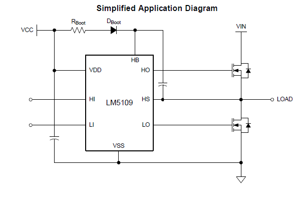
    Refer to the application diagram below and I will explain the method in which the driver operates, especially the floating high side driver.

    The first operation to understand is when the high side MOSFET is turned on the HS pin of the LM5109B driver and node called "load" will switch high to close to the VIN voltage, when the low side MOSFET is turned on the HS pin of the LM5109B with switch close to ground. With most half bridge power train topologies, you only want the high side MOSFET on or the low side MOSFET on, not both at the same time.

    The LO output is the low side driver channel referenced to VSS, usually ground in the circuit. The LI input threshold is ~1.8V rising  so an input signal from the controller will satisfy the input thresholds, even if the controller is 3.3V control signals. The LO output will switch to close to VDD when the drive input is triggered high. The HO output is a floating output driver, in that the HO output is referenced to the HS pin which is the switch node of the power MOSFETs. The HB pin is the bias for the HO output driver and is also referenced to the HS pin.

    The HB bias is usually generated with a boot diode connected from VDD to HB with a capacitor connected from HB to HS. The HB bias capacitor is charged when HS switches close to ground, and the boot diode provides a charging current from VDD. The HB voltage will be ~ VDD-Vf (of the boot diode).

    When the HI input goes high, there is an internal level shifter to interface the VSS referenced HI input to the HS referenced driver output.. When HO goes high the high side MOSFET will turn on and the HS pin will switch close to the VIN voltage. The boot diode is reversed biased and the HB to HS bias voltage is ~VDD- Vf of the boot diode. In this way the driver can drive the high side MOSFET with an HO amplitude higher than the VIN input voltage.

    Refer to the TI application note on Bootstrap circuitry selection for half-bridge configurations.http://www.ti.com/lit/an/slua887/slua887.pdf

    Confirm if this addresses your question, or you can ask additional questions on this thread.

    Regards,