This thread has been locked.

If you have a related question, please click the "Ask a related question" button in the top right corner. The newly created question will be automatically linked to this question.

LM5105: LM5105SD_NOPB

Part Number: LM5105

Hello,

I'm using LM5105SD  gate driver for implementing 3 phase H-bridge motor driver, I'm using  BSC046N10NS Infineon FET, the PWM frequency is 18kHz.

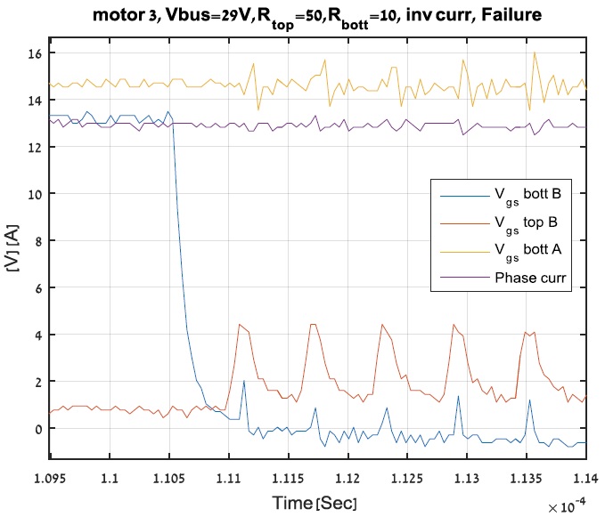
during activation of the circuit, i experienced upper FETs burns out. In the failure investigation i detected an unexplained phenomenon that the upper FET instead of start opening as expected (Vgs starts to rise) but the Vgs of the upper FET start to oscillate as well as both the Vgs of the lower FET and the other H-bridge FET's Vgs.

I attach the circuit diagram as well as recordings of both the upper and lower  FET's Vgs and another phase lower FET's Vgs.
I'll be happy to receive comments on the circuit and help finding the source of the fault.

thanks, Rami.

  • Hello Rami,

    Thanks for your interest in our driver.

    Few comments/questions/recommendations based on your schematic:

    -Bootstrap capacitor is not sized appropriately, this be at least 10x gate capacitance (4.5nF typ. from d/s) and C8 CVdd should be at least 10x this boot capacitor. 

    -47 ohms boot resistor would significantly limit charging time of bootstrap capacitor, you might consider reducing this value.

    Please refer to this copied document for bootstrap circuit sizing:

    http://www.ti.com/lit/an/slua887/slua887.pdf

    -I assume the failure is occurring with the load connected, please remove the load after updating the bootstrap capacitor to confirm normal operation.

    -Additionally, oscillations are commonly traced back to PCB layout specifically bootstrap loop inductance (connections from boot cap-HO-gate). This should be minimized as much as possible with short and wide PCB traces to avoid parasitic inductance that cause oscillations. 

    -What does HS-GND signal look like? Once load removed, please capture the following on the same phase while probing directly at the driver's pins: HO-HS (differential probe), HS-GND, LO-GND, HI-GND, LI-GND using the same time scale and zoomed-in rise/fall edges as well as and potential oscillations.

    Regards,

    -Mamadou

  • Hello Mamadou, thanks for your reply.

    I sampled my 14V (VDD-VSS) and it looks stable in all operation modes,

    My question is why to reduce the bootstrap cap ?

    with reference to the document you mentioned I calculated that the minimum bootstrap capacitance is 50nF so why couldn't i put 1uF bootstrap cap ?

    Rami

  • Hello Rami,

    I work with Mamadou and can assist with your questions. For the bootstrap capacitor and VDD capacitor we recommend the VDD capacitance of 10x the bootstrap capacitance to allow charging of the bootstrap capacitance without resulting in significant voltage drop on the VDD capacitance. If the VDD and bootstrap capacitance are equal, the VDD can drop by 50% on the initial charge of the bootstrap capacitor.

    I see on the schematic, there is a diode in series with the turn on resistance and the turn off resistance on the gate driver outputs to the MOSFET. Usually we have a resistance only for the turn on resistance and the diode and resistor for the turn off resistance path.

    I would suggest that you short CR14 and CR16 in your schematic so the driver can clamp to ground with some resistance to the MOSFET Vgs.

    Confirm if this addresses your questions, or you can post additional questions on this thread.

    Regards,

  • Hello Richard thanks for your reply,

    I used in the past this kind of cycle (with diode+res for the turn on and diode+res for turn-off) without any problem,

    What I see is that the upper FET gate signal (HO-HS) start to oscillate always in the same load current it looks like the upper  FET signal (HO) couldn't rise to turn on the upper FET, maybe the HO is in UVLO state (even though I sampled bootstrap voltage (VHB-VHS) and it was stable).

    What could be the reason that the load current make this phenomena ?

    Rami

  • Hello Rami,

    Thank you for the information. You mention the VHB-VHS is stable but can you confirm the voltage level to confirm it is not close to the UVLO point which may have some sensitivity to noise and ripple?

    One reason the load current can cause some issues is that the MOSFET Vds dV/dt usually increases at higher load currents. With higher Vds dV/dt there will be more miller charge from the MOSFET Cgd transferred to the MOSFET gate voltage which causes voltage pertubations on the Vgs.

    Can you provide some layout pictures of the gate driver and MOSFET power train to confirm if there are long traces from the driver to the MOSFET's? If there is high trace inductance in the gate drive loop, this will increase the ringing that can occur on the Vgs during the power device switching.

    If the parasitic trace inductance is the cause, one thing to try is to increase the gate resistance, which will help dampen any ringing. I would still recommend shorting the diode in the driver turn on path. Your existing circuit has a diode drop from the driver to the MOSFET Vgs, in both directions which leaves the MOSFET Vgs at high impedance below the diode Vf.

    Confirm if this addresses your questions, or you can post additional questions on this thread.

    Regards,