This thread has been locked.

If you have a related question, please click the "Ask a related question" button in the top right corner. The newly created question will be automatically linked to this question.

UCC256301: X-capacitor discharge feature getting turned on while input voltage still present

Part Number: UCC256301
Other Parts Discussed in Thread: TIDA-010015, LMV431, TL431, TLVH431

Hi!

I am trying to develop PSU that converts 220V to 48V, using a design similar to TIDA-010015. I have a problem of instability of PSU - it starts up fine, does switching fine, but may shutdown unexpectedly in a few minutes under no load or under small load (1A). Under small load it turns off faster (though there is not exact time for this). Then it shuts down similar to any fault - switching stops, output voltage drops. Interestingly, it does not get turned on after. output voltage stays down, thougn 400V from PFC is present and UCC256301 kind of tries to turn on - I see voltage rise on VCC pin, I see long pulse on LO pin, but switching does not start again.

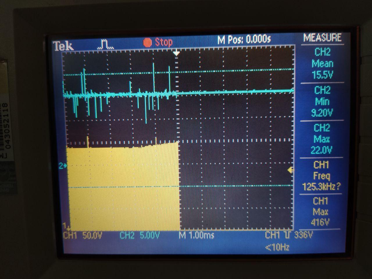
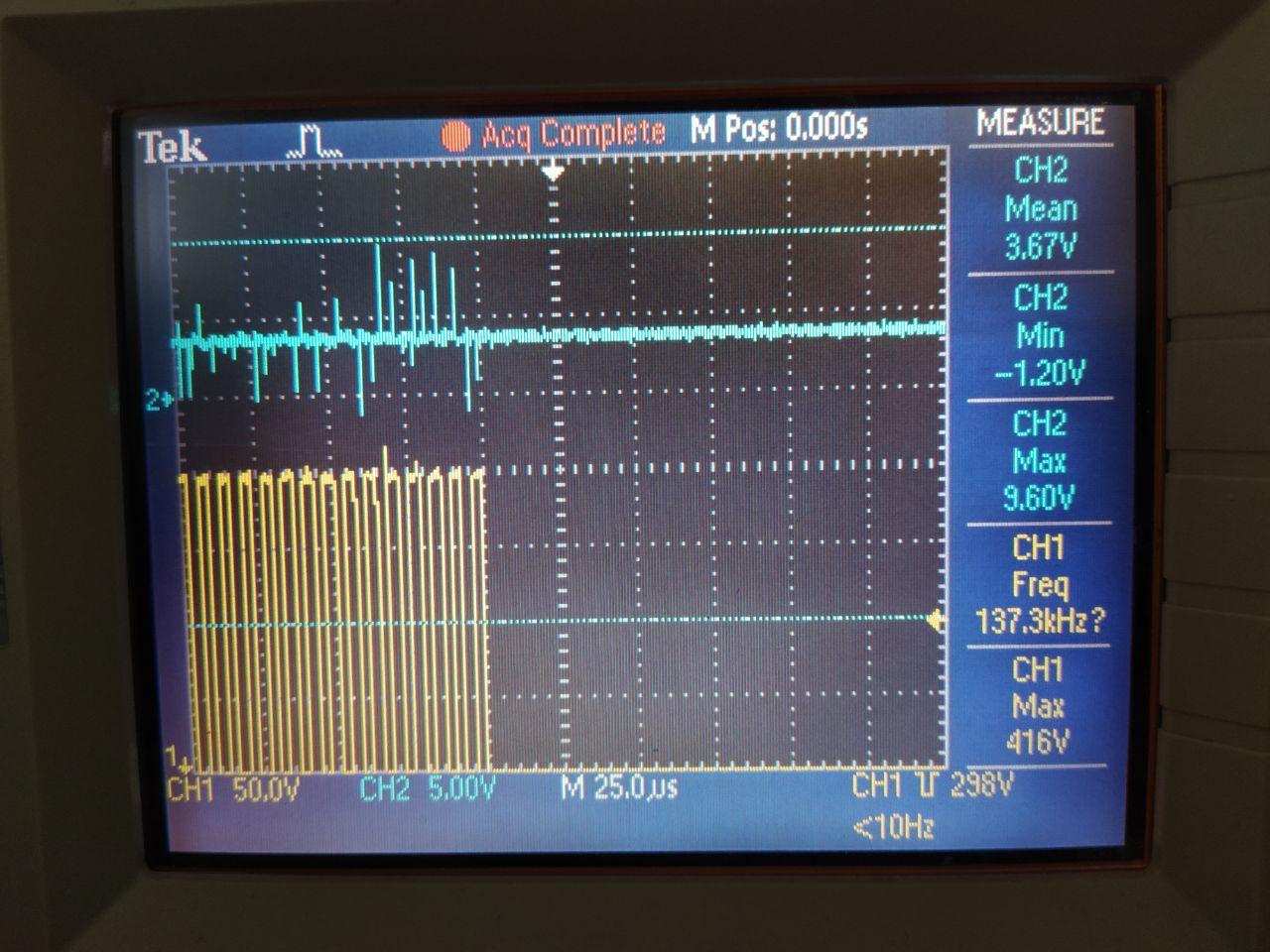
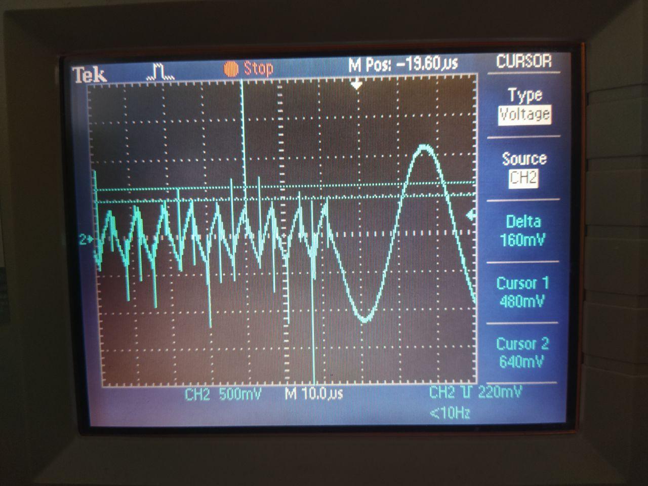
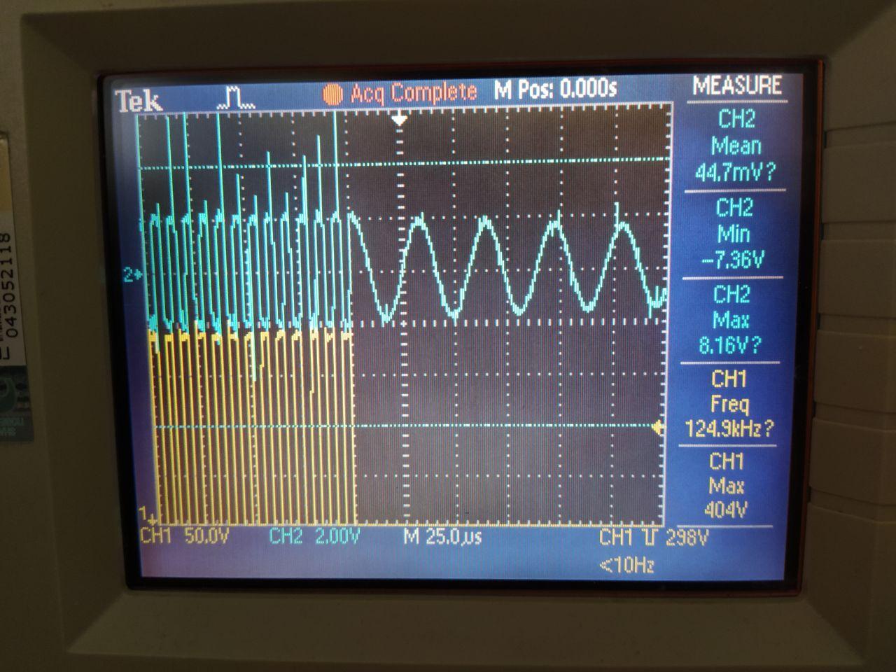
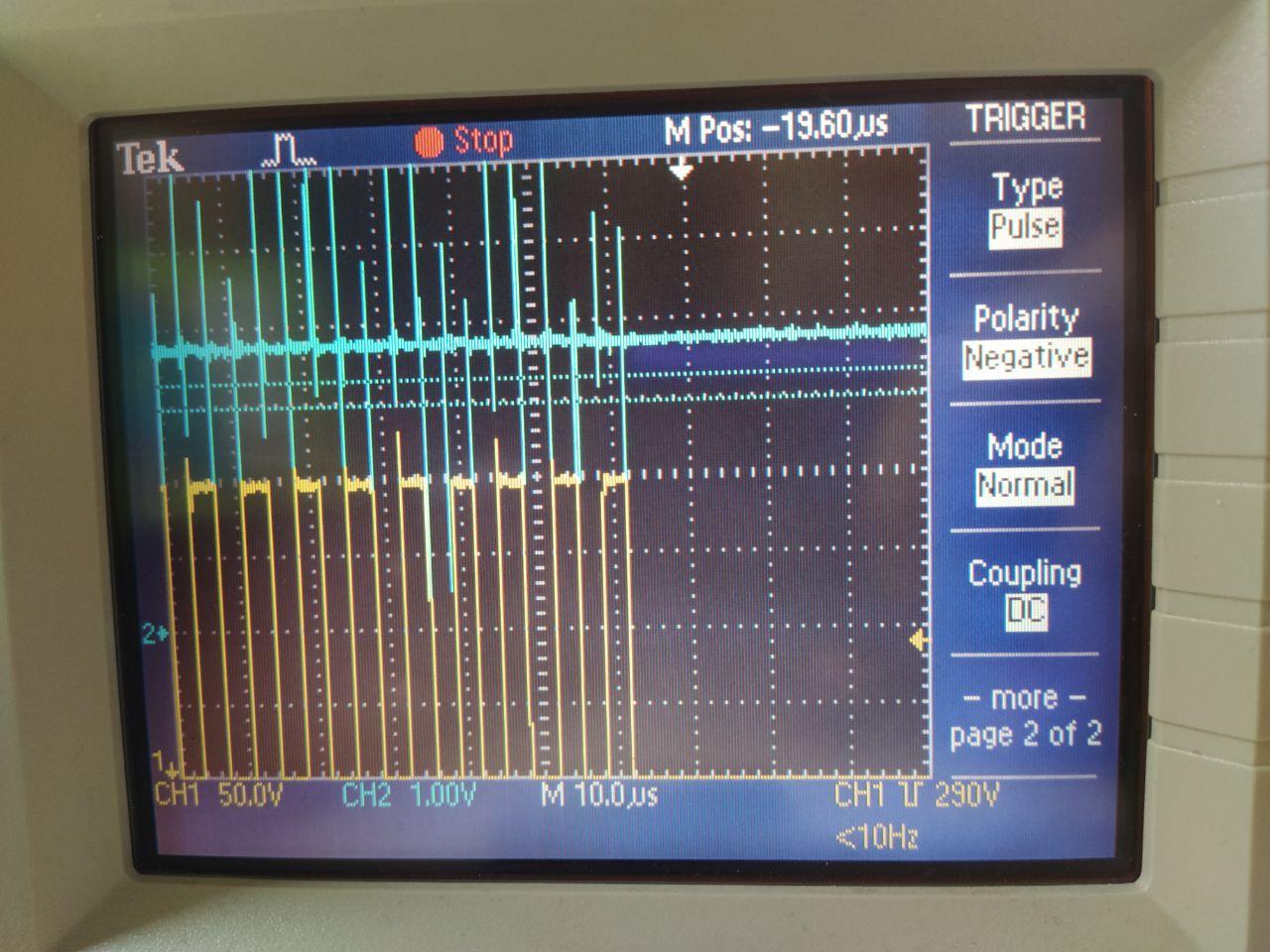
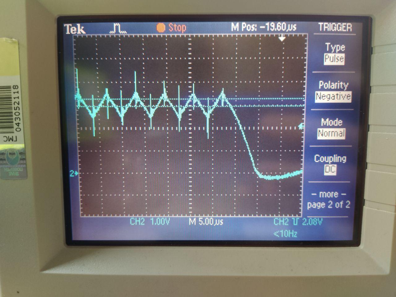
When in such condition UCC256301 stops switching, I also see a sudden change in HV pin series resistor current (measuring voltage on one 1.5 kOhm resistor of three resistors) - curent from less than 1 mA will change to about 10 mA. I can't be sure if it happens before the switching stops, at the same time or right after as I don't know how to synchronize switching with this current. It happens at around the same time, so I assume it to happen right before switching stops.

My undestanding of what's happening: in one random moment of working UCC256301 somehow decides that input voltage 220V absent (even though it is still present) and starts discharging X-capacitor, almost instantly overheats and goes out with OTP fault (wild guess). After that it can't restart due to that overheating, which is renewed by charging VCC voltage (and current through HV pin). I can't verify overheating due to being afraid to short something on PCB without a way to fix firmly thermocouple on UCC256301.

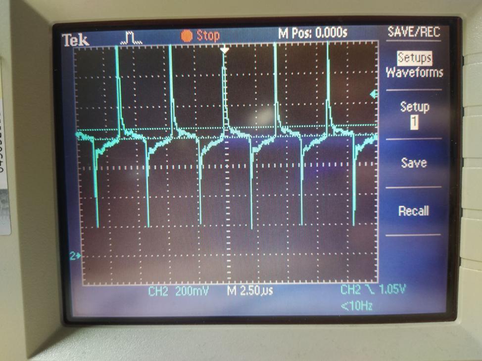
I also see zero crossing on HV pin (measuring voltage between HV and GND) while UCC256301 is still switching, happening once in around 700 ms (due to the test current, which is happening with that period, according to datasheet). But if I look at the current on one of HV pin series resistors, I see always the same (kind of) triangular signal as on the left side of the picture above. But perhaps the change in current once in 700 ms is just too small for me to see.

So, I guess, my questions are:

1. Is there any activity on HV pin during or after any FAULT condition? Just so we could rule out the possibility of X-cap discharge function not being the cause of PSU shut down.

2. What could be the reasons for X-cap discharge function happening wuth input voltage still present? If that is the case at all.

I am also aware of other versions of UCC25630, which do not have this X-cap discharge function, but it would be nice to have it working as it is, without changing to other IC.

  • Hello Aleksey,

    Thank you for your interest in the UCC256301 LLC controller.

    I discussed this issue with another engineer and he suggests that the high HV current that you measured may be due to restart of the IC after VDD voltage fell to the UVLO shutdown threshold. You say your design is "similar" to TIDA-010015.  This design uses 3 1K resistors in series with HV, your design uses 3 1.5K resistors.   

    This deviation does not account for the restart, but I mention it because there may be other difference between the TIDA design and your design that may be pertinent to the issue. Is it possible for you to provide an up-to-date schematic of your LLC section?  There may be more clues as to what is happening there.

    If you don't wish to make it public, you can send it to my email: ulrich_goerke@ti.com

    Meanwhile, please probe the VDD voltage and see if the spike in HV current corresponds to the UVLO threshold of the VDD input. If it does, we'll need to find out why the VDD capacitance is inadequate to keep Vvdd above this threshold. 

    Regards,
    Ulrich 

  • Hello Ulrich!

    Thank you for answer. I sent the schematic to your email. There are some changes to it, marked by crossed out components or value of component. Also note that R78 (RF1 for TIDA-010015) is shorted out now. Also at the time of writing this post resistors R1-R3 (R10, R22, R31 for TIDA-010015) were 1.5 kOhm, but after that I changed them to 1 kOhm each. Following pictures were taken with R1-R3 = 1 kOhm. Also I forgot to change the value on schematic of R43 (R43 for TIDA-010015) - it is actually 182 kOhms, sorry for the mess.

    I didn't really understood what you meant by "VDD" - was it VCC pin or RVCC? Only RVCC has UVLO, as far as I know. So I measured both, there seems to be nothing wrong with them.

    Blue signal is VCC voltage at the time when switching stops. Yellow signal is SW voltage.

    Blue signal is RVCC voltage at the time when switching stops. Yellow signal is SW voltage.

    Measurements have different time scales, but I think that voltage drop enough for UVLO would be noticeable in both scales. There are some spikes on the VCC and RVCC voltages that are probably due to the probes of oscilloscope (I noticed earlier that if i take measurements of, for example, ISNS voltage, it has multiple spikes on it if I measure both ISNS and SW signals, but has far lesser spikes when measuring only ISNS voltage).

    Blue signal is BLK voltage at the time when switching stops. Yellow is SW voltage.

    For this measurements i loaded the PSU for 1A and waited for about 15-20 seconds until switching stopped.

  • Adding a measurement of ISNS for PSU that stopped switching at the load of 1.1A.

    Adding a measurement of BW for PSU that stopped switching at the load of 1.1A. Both pictures are the same, one is just with turned off channel 1. Yellow - SW, blue - BW.

  • Hello Aleksey,

    Thank you for providing your schematic by email.  I se that it is very similar to the TIDA010015 except output voltage is increased to 48V.  
    I assume that the power level is still the same as the TIDA design, at 480W, which means the output current would be cut in half.
    (I further assume that the transformer T1, although drawn the same as in the TIDA schematic (including incorrect polarity marks), has been modified for the higher voltage, lower current of your design.) 
    Your latest waveforms indicate that the converter appears to be happily converting, then just stop suddenly.  I agree, the VCC, RVCC and BLK voltages all look good.

    In your design, the output current sense circuits involving DA3 and DA1 use the same supporting component values as in the TIDA. Specifically, R8, R23, and R24 set up a ~0.1V threshold to trigger driving V1 optocoupler to adjust the LL burst mode threshold. Based on DA3 gain of 200V/V and 0.0005R sense resistor, this threshold would be met at about 1~1.1A output current.     

    It is my suspicion that your R17 may not be 487K, but something much less and when Iout = ~1A, V1 is driven to adjust LL, but I think it is being pulled low enough to shut off operation.  This does not completely match your original symptom descriptions for loads < 1A or no-load, but it may be possible that switching noise or some other effect serves to trigger this threshold. 

    I suggest to depopulate R17, to make sure this circuit has no influence on the LLC controller.  Then, if the LLC converter operates successfully for long periods at higher current, you can investigate the current-sense circuits to debug them.

    If removing R17 does not improve things, then we'll have to think further.  For instance, from the primary-side "point-of view", all of the thresholds and protections are based on the 24V/20A of the TIDA design.  WIth your 48V output, all these thresholds and protections will occur at 1/2 of the current of the TIDA design (except for opto V1,which has direct sensing at R37).  If this is not what you intend, then some primary-side parameter adjustments will be needed.

    Regards,
    Ulrich

  • Hello, Ulrich.

    Thank you very much for your help with this.

    Yes, the DA1, DA3 circuit does exactly that in practice (adjusting burst mode to 1-1.1A). As you can see in pictures below, removing R17 (R70 in TIDA-010015) did not play any role in changing LL/SS voltage.

    I also remember about current threshold, but for the time being it should not matter, because with components that are placed in circuit now I should be able to get about 7.5A of output, but can't get it working to even half that current.

    Sometime ago among other problems I already met this issue with current of 1.7A approximately. When I changed R22 (R3 in TIDA-010015) to 150 Ohms, this issue started occuring at around 3A. But while I was debugging it, PCB was fried from working for 7-8 minutes at that current (I waited for the issue to happen). It was with different VT3-VT4 (Q2-Q3 in TIDA-010015), when R19 (R38 in TIDA-010015) was 330 Ohms, and perhaps with another PCB, hard to tell now. I had problems with overshoots on VT3-VT4 (Q2-Q3 in TIDA-010015) due to diodes reverse recovery damage, first "solved" with enlarging of value of R19 (R38 in TIDA-010015) (which probably led to heating problem), that really solved with changing MOSFET to the ones with lesser reverse recovery charge. Anyhow, at only slightly different version of my PCB I had way more stable operation at the same load. And also important fact, that by adjusting ISNS resistor we can change current at which circuit operates successfully, though it happens far from predictable values.

    Perhaps noise could be the reason for ISNS tripping? Filtering capacitor is placed quite far from UCC256301 ISNS pin, but if placed right on top of UCC256301 changes nothing. Also tried putting 22 pF capacitor on top of UCC256301, but didn't see any change, still stops switching prematurely. 

    OVP protection from BW does not seem to trip, BLK seems normal, VCR does not exceed its maximum voltage (look at pictures below), VCC and RVCC are good. My thoughts that it could be:

    1. Some feedback problem which leads to UCC256301 stopping switching. Feedback I can't really debug, because TL431 starts oscillating if I try to measure something at R12, R42, R41 (due to noise from wires used to connect oscilloscope to those points or from probe's capacitance). Also if i try to measure signal at R87, output behaves very strangely (similar to oscillating of TL431 probably). Though I can measure FB signal just fine. I would probably like to change TL431 to LMV431, which needs lesser amount of current flowing through it to operate reliably, but it will lead to many changes in feedback circuit, so I don't want to do that without absolute necessity.

    2. Strange activity on HV pin. Perhaps, as I first suggested, X-cap discharge gets tripped somehow when 220V are still connected, which leads to overheating of UCC256301, which in turn leads to OTP tripping and stopping of switching? It is the only thing (in my mind at least) that can explain the fact, that, once stopped, switching will not reoccur while 220V are still connected (though VCC gets charged through HV pin all over again and I even see long pulse at LO pin, which usually preceeds switching start).

    3. Noise tripping OCP1 or any other FAULT.

    I am concerned about switching not starting after it stopped as much as I am concerned about it stopping. Perhaps it is a hint, which could lead us to fixing this issue. Particularly considering the fact, that if switching stopped not because of that issue (for example, OCP1 tripping during first few cycles, which happens often), it is then restarted after 1 second.

    I am loading PSU using electronic load AKTAKOM AEL-8321. Measuring signals with oscilloscope Tektronix TDS2012.

    LL/SS (blue), SW (yellow) at the moment when switching stopped, which happened at 0.9A (I was slowly turning load up) with R17 still attached.

    LL/SS (blue), SW (yellow) at the moment when switching stopped, which happened at 1A after 30-60 seconds of work.Happened with R17 absent. At other time at the same conditions stopped switching at 0.2A of load.

    VCR signal at the moment when switching stopped, which happened at 0.6A. R17 is absent.

    Regards,
    Aleksey.

  • Also, how can I estimate necessary value for resistor R42 (R47 in TIDA-010015)? I know that the purpose of this resistor is to provide current for TL431, needed for proper regulation. But how do I choose an exact value? In this topic (https://e2e.ti.com/support/power-management/f/196/p/757072/2821130?tisearch=e2e-sitesearch&keymatch=ucc256301%252520tl431#2821130) it is told that the value is chosen so that voltage across optocouple LED pins is 0.5-0.6V, but why exactly this value? 

    In TIDA-010015 this resistor has value of 6.04 kOhms, in the topic above it is chosen to have value of 500 Ohms (for TL431, not for TLVH431), so how exactly should it be estimated? I am concerned that this resistor could be to blame for my problem of instability of PSU (by not giving enough current to TL431).

    Regards,
    Aleksey.

  • Hello Alexsey,

    I'm sorry I was unable to answer for several days.

    To answer your last questions first: the value for R42 can be relatively loose.  It does not need to be exact, but it needs to be low enough to provide the minimum bias current to the shunt device.  The value will differ depending on the minimum current for each individual device, which vary considerably.   In my advice on this topic that you reference, the resistor value is not chosen to make the opto-diode equal to 0.5V, it is chosen for when the opto-diode voltage is 0.5V.  

    This is because at 0.5V, insignificant current flows through that diode. In most feedback systems using shunts and opto-couplers like this, full power is delivered when the feedback current is zero, or near zero.  That means the shunt anode voltage rises high enough to cut off current through the diode.  Yet the shunt still needs bias current, so there has to be a path around the diode.  If all bias current goes through the diode, the opto output current will reduce power and the output voltage will not receive the full power it needs to regulate Vout at full load. If the shunt rises high enough to cut its own bias current, it losses "sanity" and anode voltage falls.  This turns it back on again and it rises to cut off the current, leading to the instability that you found.

    0.5V across the diode is enough voltage across R42 to provide the shunt with its needed bias current while the current through the diode at 0.5V is not enough to generate collector current and pull the feedback current to the primary controller down. You can reduce R42 to have a little more current than the minimum, but not so much that the voltage drop across R41 becomes to high to allow for its own regulation variations.  I hope this clarifies the reasoning for R42.

    Back to the main problem; I think I am inclined to agree with you that OTP must be the most likely reason for the shutdown and eventual restart after a cool down period.  And your observation that HV appear to perform an X-cap discharge needs to be investigated in more detail.
    If lack of variation of HV current during the x-cap test triggers the X-cap discharge function, then maybe something in the HV path is not working correctly.   

    Try replacing VD10 and VD11 with new diodes, maybe even different part numbers.
    For temporary test purpose only, try adding a parallel resistance from netA straight to primary GND.  (Make sure it can handle the power dissipation). The purpose of this is to put a constant load on the two diodes to make sure netA voltage does go to GND each half-cycle.  Then see it the unwanted discharges still occur.

    Another possibility is that that particular LLC controller got damaged somehow during previous testing and fails sporadically.  If you have another unused UCC256301, please try to replace it with the new one and see if the problem still happens or not.

    Regards,
    Ulrich

  • Hello, Ulrich.

    Thank you for answering. I tried replacing VD10-VD11 with differend diodes, but nothing changed. I also tried soldering in a switch between diodes and resistor R3 so that I could cut off this path entirely once UCC256301 started switching, but still no luck. With VD10-11 cut off during switching, UCC256301 still continues switching, but under load it still fails eventually. So, apparently, HV pin activity is an after-effect of switching stopped, not it's reason. I'm thinking that UCC256301 could somehow reset, which would cause switching to stop and HV pin to start sinking current to VCC pin again. Though it is still interesting that switching won't start again after stopping.

    I also tried replacing UCC256301 with another one (though from the same batch) quite long ago trying to solve this problem, but nothing changed. 

    And I measured the temperature of the whole board while it was switching. Turns out VT10, VD4, R44 circuit was rapidly heating up even under no load, That would explain everything: under burst mode it would heat up a bit less than under full load, so stopping switching under load of 1A would perfectly fit the picture - this circuit would heat up, stop supplying VDD, which would cause the rectifier on the output stop working. But (sadly, there's always a but) when I changed VT10 to bigger NPN (TO220), I got way more reasonable heat up, though under load UCC256301 stopped switching nevertheless. I measured temperature of both sides of PCB at the moment when switching stopped and got no more than 40 degrees Celsius.

    For now I don't have any other ideas but to try to debug feedback circuit.

    Again, thank you for your help.

    Regards,
    Aleksey.

  • Hi Aleksey,

    Something you wrote made me take a look at your schematic again.

    This time I noticed something different.  On the primary side, you have the GND symbol as a pointed triangle. On the secondary side, your GND symbol is a flat rounded "foot".  But you have two components between R41 and R100 at the opto coupler (V2) that have no reference designators and the GND on them is a flat line.  These are a 20V Zener and a 100nF cap to clamp the bias voltage to the TL431 (DA2). 

    Are these parts actually populated, and do they both go to the secondary GND, or only to their own local "GND".

    I am hoping this drawing discrepancy may account for the higher-load shutdowns, where at light load, the TL431 draws enough current to keep its cathode voltage within spec, but as load increases, the shunt current falls and Vk rises above the TL431 spec.  Then it "fails" temporarily.

    That's all that I can think of at the moment.

    Regards,
    Ulrich 

  • Sorry for the mess, the ground symbol of course should be  "a flat rounded "foot"". Physically ground connection of those components without reference designators is connected directly to anode of TL431 by wire. They were added after the manufacturing of PCB, so in schematic CAD they are made not as a component, but as a drawing of a few lines, which is the reason for them not having reference designators and the GND symbol drawn the wrong way.

    Could TL431 circuit be to blame for PSU shutting down? After all, the resistors around it (the ones that define current through TL431 and optocouple) are selected empirically, without real calculation. 

    Regards,
    Aleksey.

  • Aleksey,

    The value of R42 was discussed a few sessions above. It is possible that your particular TL431 requires a bias current closer to the maximum value of 1mA to function properly.  To "guarantee" that, you can reduce R42 to 510R or 470R.  This would be necessary at higher loads when the opto-diode current is reduced or cut off.

    R41 has a maximum value such that you can get the minimum bias current (through R42) plus the necessary opto-diode current to satisfy FB current at no-load (iFB = 85uA).  The lowest typical CTR of the TLP181 (now in "End of Life" status, by the way) at Ic = 85uA is about 35%, so needs at least 240uA diode current at no-load.  Maximum R41 value must provide 1mA bias plus 0.24mA diode current when Vk of TL431 is lowest (~2V), so (20V-2V)/1.24mA = 14.5K.  As it is, R41 = 12.1K meets this max criterion.  R100 needs to provide the same TL431 current plus bias for the 10V Zener.  Accuracy is not important, so let's say 1mA is enough, then (48V-20V)/2.24mA = 12.5K maximum for R100.  8.05K meets this criterion.  So those values should not hamper proper shunt operation.  

    All of this is on paper, of course, and although the schematic seems to work, the real board doesn't.  It is possible that one of the components is not what is shown on the schematic diagram. The wrong value may work at light load, but not at heavier loads.  Or thermal expansion might make or break a cracked connection or solder joint.  I'm afraid that all of these possibilities need to be checked out, which is a tedious process.

    Eventually, we'll find what is causing this problem.  Each little sub-circuit needs to be checked to verify that it behaves as expected at all the different operating conditions.  Since you are unable to increase load beyond ~1A, something is not behaving properly as this "limit" is approached. You may be able to find a circuit that is reaching a clamp or limit level (either in current or voltage) that should not be there.

    Regards,
    Ulrich

  • Hello Ulrich,

    Thank you for your help, your calculations really help to make it all clear.

    Changing R42 to 470 Ohms shutted off all regulation at all - optocoupler didn't have enough current and UCC256301, thinking no power was delivered to output, maxed out power delivery, so the output received almost 100V of voltage. OVP not turning on is also an issue, but that is not the point right now. I recalculated and repopulated R32 to 47.5k, so that OVP would trigger at about 70V, but even after that if I met similar problems, OVP sometimes would not trigger.

    So I tried to change the feedback schematic a bit and switched to a LMV431 instead of TL431. DA2 is now LMV431, R42 = 6.04k, R41 = 24.9k, Zener has the value of 11V, R100 = 27.4k, R43 = 301k, R12 = 8.25k. That was on another PCB, so I have previous schematic ready to compare, if need be. After that I got almost the same results as before - PSU would work fine without load, but would stop switching shortly after turning the load on. I measured current through R87 and got the following results.

    Without load:

    With load of approximately 1A (a bit more, about 1.1-1.2A):

    I'm not much concerned about no-load current through R87 since it works for now, but current through R87 when PSU is loaded is a bit strange, as I think. The way I understand it, compensation circuit of C49, R13, C13 should slow down reaction of DA2 to switching pulses, so that DA2 would react to more slow change of voltage due to loading of output. So, if I understand it correctly, DA2 should not react to switching pulses in such big current spikes. Is it really abnormal to see such spikes, or I just don't understand it?

    Regards,

    Aleksey

  • Hello Aleksey,

    Current spikes like you see above ( in your last post) are abnormal, however, I'm not sure that they are really there.  Since you are probing approximatively one volt signal on a 200mV/div scale, it is probably noise pickup of nearby high-voltage switching that is superimposed on the current signal.  I can't imagine current of that magnitude and frequency content passing though the optocoupler transistor.  

    Please follow the probing technique shown on page 5 of this App Note to minimize noise pickup: http://www.ti.com/lit/an/slea025a/slea025a.pdf?&ts=1589504523542.

    I'm going to try to find an LLC expert who maybe can provide better help than I am able to, to solve this problem.  It seems there is something that both of us are missing.  It may take a day or two for him to come up to speed on the issue.

    Regards,
    Ulrich

  • Hi Aleksey,

    Could you please try adding a 1nF capacitor between ISNS and IC gnd and see if the converter continues to stop switching? Place the capacitor as close as possible to the ISNS pin. If you continue to see the converter stop switching, please increase the ISNS bypass cap up to 2.2nF. There is seems to be some high frequency oscillation in the ISNS signal and it might be messing up the ISNS polarity detection of the ZCS protection function.

    Best Regards,

    Ben Lough

  • Hi Ben,

    That seems to do the trick - I added 1nF capacitor across IC's body between ISNS and GND and PSU seems to work way more stable after that. It also had a problem of turning on from 5-6th time - it slowly accumulated output voltage by a few volts a try until it eventually started, placing a capacitor cured it from that problem. For now I had a success of working for 2 and 5 minutes without a fault, turning off PSU myself to see if something heated. Sometime ago I tried adding 22 pF the same way but it did not help the issue. In UCC25630x Practical Design Guidelines it is said that: "Too much low pass filtering on ISNS may result in a delay in resonant current polarity sensing and error in overcurrent protection.", so I did not dare to add more capacitance. Can you give some hints about how much is "Too much low pass filtering"?

    And thank you very much!

    Regards,

    Aleksey.

  • Hi Aleksey,

    What I normally do is compare the resonant current to the ISNS waveform and make sure there isn't significant phase shift between the two waveforms. If there is excessive bypass capacitance the ISNS waveform will be significantly delayed and will impact the OCP 2/3 detection. Most designs will tend to have few pF up to ~1nF depending on how much filtering is needed to keep the ISNS signal clean.

    Best Regards,

    Ben Lough