This thread has been locked.

If you have a related question, please click the "Ask a related question" button in the top right corner. The newly created question will be automatically linked to this question.

TPS25200: How to use TPS25200 for reverse Voltage Protection

Part Number: TPS25200
Other Parts Discussed in Thread: TPS2500, , TLV62585

Hello Team ,

We are planing to use TPS2500 IC in our board for over voltage and over current protection.

But we need a reverse voltage protection with this IC .

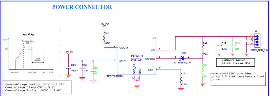
We are planing to use diode on Enable pin that will disable this IC in reverse voltage 

But this will protect the Vin pin or not is a issue 

Please share  if you have any another solution for reverse voltage.

Use attached image for your reference.

  • Hello Team ,

    one more thing  we do not want to use diode in series at Input pin or vin pin due to voltage drop across the diode and current rating of diode.

    Thanks ,

    Shubham

  • Hi Shubham,

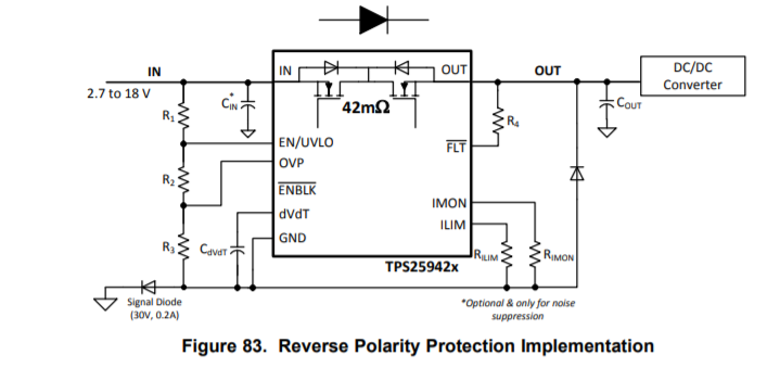
    When a reverse voltage is applied at the input, this means the IC is subjected to reverse polarity. The signal diode in the GND terminal path ensures that device is not functional during reverse polarity conditions and internal FET blocks the reverse path.

    You can test this circuit before using this on your board.

  • Hello Praveen,

    Thanks for the support.

    If we are design the system for 2.3A then we can use the diode on ground path with 0.5A rating or need need to use higher rating diode.

    Because total current return path will from this diode so may be we need to use 3A diode on this path '

    please suggest your input on this 

    Note: we do not want to use higher rating diode. 

    Thanks,

    Shubham

  • Hi Shubham,

    The load current doesn't flow through the signal diode that we have added between the IC GND point and System GND. The current flowing in the diode will only be the device quiescent current,  IQ  + Current through resistor dividers. 

    That is why the rating of the signal diode in the image is 30 V , 0.2 A 

  • Hello Praveen,

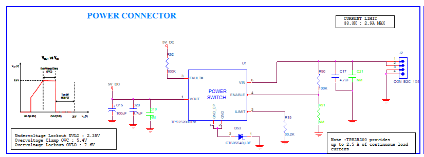
    -We are planing to use TPS25200 this logic will work this this part ????

    -Can we remove the D52 from EN pin.

    -How the D53 will work in normal and reverse voltage.

    -Please review the attached image and let me know any issue is their.   

    Thanks, 

    Shubham

  • Hello

    We are using below option .

  • Hi Shubham,

    This configuration should work for Reverse Polarity Protection. However, we recommend you to test this circuit before implementing on your system.

    For reverse polarity protection to work with a signal diode in the IC's Ground path, the IC needs to have Reverse current protection feature,

    • TPS25200 blocks reverse current only when the device is in OFF condition. On the other hand, TPS25942x/4x family of devices block reverse current in both ON and OFF condition.
    • As TPS25942x/4x family of devices have more robust reverse current blocking capability, I would suggest you consider these devices for reverse polarity protection in youor design.

  • Hi Praveen,

    I have a few questions-

    1. We can't go with the TPS25942x family due to cost concerns but as we are using TPS25200 with diode, can we use one more diode at Enable Pin as well?

    So enable Pin will not enable the IC during the reverse voltage condition and this device protects the reverse current in OFF condition. 

    Can you please suggest?

    2. TPS25942x family has two FETs inside but here in TPS25200 have one single FET inside so do you think that this diode may work in reverse protection? 

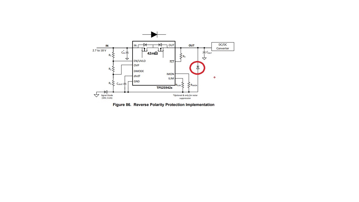
    3. For TPS25942x family, there is one diode connected at Output as well, what is the purpose for that?

    4. For this Circuit, how the Ground Potential for the IC GND pin would be higher than the diode voltage drop during the normal condition?

    1. Do you see any issues during normal functioning?
  • Hi Saumil,

    1. A diode is not required on the Enable pin. The device will not be enabled when there is reverse polarity.

    2. TPS25200 actually has two FET's internally connected in back to back fashion. Hence, there would be no reverse current flow when the device is disabled.

    3. The diode connected in the output is a schottky diode. It is used for suppressing negative voltage transients at the output which can be generated due to inductance in the output path during Fast-trip events. Please refer to section '11.1 Transient Protection' in the datasheet for more information. 

    4.  As you said the IC reference potential will be 'diode drop' higher than the system GND potential. You need to refer the components related to the IC to the IC reference. By doing so, there will be no change in the current limit but EN/UVLO and over voltage protection thresholds will be shifted by the diode drop voltage. There should be no other issue in this configuration.

    We have not tested this device for reverse polarity protection using a diode. So, we recommend that you test the circuit for all  your system use cases before implementing in your system. Due to the current COVID-19 situation we are not able to access our labs and help you in testing.

    Thanks for your understanding!

  • Hi Praveen,

    Thanks for the detailed answer to each question during this COVID situation.

    It is really helpful.

    Now regarding the Point No -4:-

    4.  As you said the IC reference potential will be 'diode drop' higher than the system GND potential. You need to refer the components related to the IC to the IC reference. By doing so, there will be no change in the current limit but EN/UVLO and over-voltage protection thresholds will be shifted by the diode drop voltage. There should be no other issue in this configuration.

    Saumil - So you mean to say that Enable, UVLO, and Overvoltage Protection would be shifted to +0.3V if the diode drop is 0.3V, correct?

    Now this TPS25200 is clamping the Overvoltage to 5.4V then it will be also shifted to 5.6V? We are using TLV62585 after TPS25200 and that has input voltage range limited to 5.5V. The diode that we have used has a 0.3V drop at 100mA and it has a Forward voltage drop less than 0.1V with less current.

    Please see below is the updated schematic and please let me know your comment on that.

  • Hi Saumil,

    • Yes, now the over voltage clamp will be shifted by the diode drop.

    The maximum voltage that the TLV62585  can handle is 6V as per the datasheet. The max clamping voltage of TPS25200 is 5.55V

    So, the diode drop should be < 0.45V (6V - 5.55V)

    • The enable voltage will be = Vin-diode drop * (R91/(R90+R91)) 

  • Hi Praveen,

    Thanks for your detailed answer.

    Ok, We are planning for Power Adapter that will have Max output is 5.5V so that will also help.

    Just to confirm, for the Overvoltage Clamp, it will be adjusted to = 5.55V + Diode drop, is that correct?

    Thanks

    Saumil

  • Hi Saumil,

    The TPS25200 clamps the output voltage with respect to its reference GND. Here as the IC GND is diode drop voltage above the system GND, the otuput voltage w.r.t system GND would be 5.55V + Diode drop

    Do let us know if you have any other questions ?

  • Hi Praveen,

    This is ok.

    It seems resolved for now and no further question.

    Thanks

    Saumil