This thread has been locked.

If you have a related question, please click the "Ask a related question" button in the top right corner. The newly created question will be automatically linked to this question.

TPS546D24AEVM: How to set output voltage higher than 1.5V?

Part Number: TPS546D24AEVM
Other Parts Discussed in Thread: TPS546D24A, TPS546D24

Hi there,

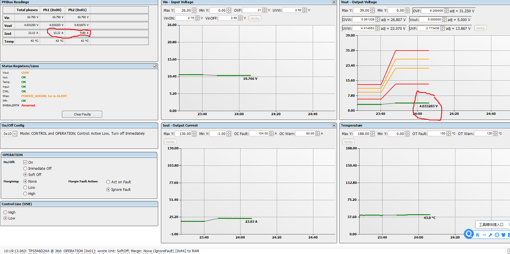
Does TPS546D24AEVM board could output a voltage  higher than 1.5V? The inductor value on EVM board is 150nH, Does the Output support 0.6 V to 5.5 V at 80 A?

When I set the output voltage using Fusion Digital Power Designer. There have  a note: You must enter a number betweent 0 to 1.5.

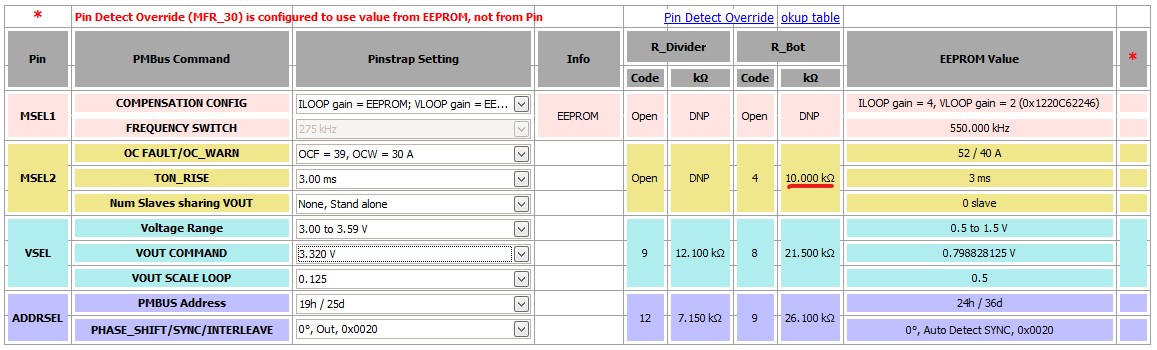
I changed the Pin Strapping. But there was nothing happend. How to set these commond to EEPROM?

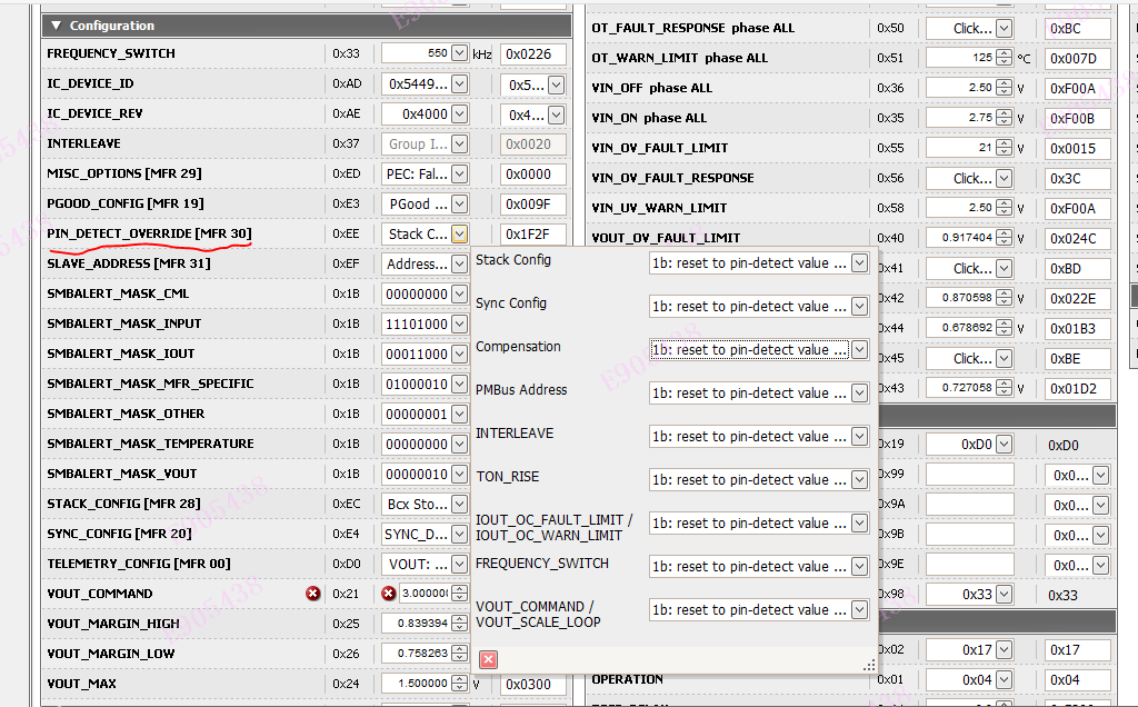
Here is Pin Strapping.

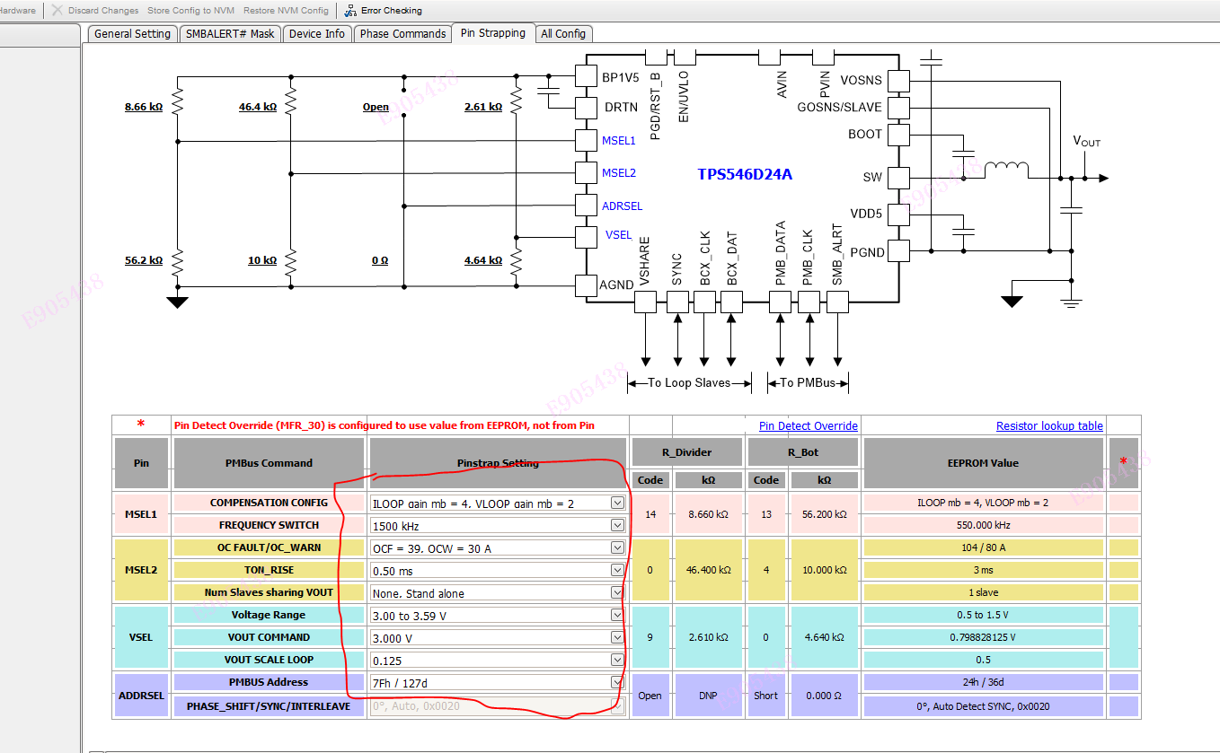
Pin_detect_override is set to 0x1F2F.

Regards,

Ricardo

  •  

    The range of the output voltage is limited by 2 functions

    The VOUT_MAX function clamps the output voltage programmable range

    the VOUT_SCALE_LOOP function sets the internal divider between the VOSNS to GOSNS remote sense amplifier and the internal reference voltage.  Since the internal reference voltage is limited to 0V to 0.75V, to get a voltage higher than 1.5V, you will need to change VOUT_SCALE_LOOP to 0.25 or 0.125 to enable output voltages upto 3.0V or 6.0V respectively.

    The VOUT_SCALE_LOOP connect is read-only while the output voltage is enabled, so you will need to disable the output voltage before changing VOUT_SCALE_LOOP.  Since VOUT_SCALE_LOOP is loaded as part of the Pin Detection, you will want to clear the VOUT_COMMAND bit in PIN_DETECT_OVERRIDE if you intend to store the VOUT_SCALE_LOOP value to NVM.

  • Hi  Peter,

    Thanks for you support. That works now. 

    But I still have some other problems.

    Question 1. The output voltage was set to 5V. After writting config to hardware. The real output voltage couldn't exceed 4V. Current on Ph#1 and ph#2 are differnet. The results are as following:

    Is there any register that I didn't set?

    Question 2: How to set stand along output? I want to set ph#1 or ph#2 to 30A, but not 2 phase parallel.

    I changed pin strapping setting. While, it may not correct.

    Questiuon 3: When I set vout scale loop to 0.125 and switching frequency to 1.5MHz.  I get a wide range output voltage form 2V - 6V. But if I want get another output voltage range, like 0.25V - 0.8V. I have to disable the output voltage, then change vout scale loop and switching frequency. At this time, the Vout will drop to 0V. I don't want the output voltage drop to 0V. In my application, the output voltage is:0V jump to 3.3V,then jump to 2.5V,then jump to 0.6V. Not 0V --> 3.3V --> 2.5V --> 0V -->0.6V.  So, do you have any idea to solve this problem?


    Regards,

    Ricardo

  •  

    First, I would recommend installing the latest version of the FUSION Digital Power Designer - https://www.ti.com/tool/FUSION_DIGITAL_POWER_DESIGNER

    Second, at 1.5MHz, the minimum off-time of the TPS546D24A is going to limited the available duty cycle, which will limit the possible output voltage.

    That is likely why the ouptut voltage is getting railed at 4V and why the current sharing is not working, the PWM can't support the ouptut voltage.  If you reduce the switching frequency to 1.1MHz, you should be able to adjust the ouptut voltage over the full range with a 10V input.

    For Pin Strapping, the selection you have highlighted is for a Single Phase Output with no slave devices.

    For Single Phase (1 device generating 1 ouptut) with a 30A current warning, 39A current limit, and 3ms soft-start time, you would select a 10kOhm MSEL2 resistor to ground.

    For adjusting the output voltage, it is possible to set the VOUT_SCALE_LOOP = 0.125 and VOUT_MIN to 0V, then adjust the output voltage from 1LSB to 6V.  To regulate to very low voltages, you will want to change the VOUT_OV_FAULT_RESPONSE and VOUT_UV_FAULT_RESPONSE to "Continue Operating without interruption" as the the relative comparators could generate false triggering of OV and UV levels with the internally sensed voltage (VOUT x VOUT_SCALE_LOOP) is so low.

  • Hi Peter,

    Yes, the minimum  Toff(400ns) limited the maxmum switching frequency. For our application, The max input voltage is 10.5V, η is 0.8 in the worst condition, and max Vout is 4.5V. So The max switching frequency is 1.1MHz.

    After a series testing. I still have some questions.

    1.

    L(min)=[Vout*(Vin-Vout)] / [ΔIL*fs(max)*Vout]=234nH.

    max output current is 30A, 1/3 output current is chosen to ΔIL.

    So I think the 150nH inductor on the TPS546D24AEVM board is not a good choice for our application. Maybe a 300nH inductor should be chosen at there(4.5V output).

    2.

    Here is our real PCB structure.

    Because our PCB have not completed yet. So I using a 50cm wire to connect EVM and load. The parasitic inductance is about 1uH, parasitic impedance is about 11 mOhms.  I set the output voltage to 3V. The output current is about 20A. Then, turn on. At this situation. It triggered the over current protection.

    After reducing wire to 10cm. The OCP trigger wasn't occured.

    Is it safe if I turn off the OC_current_fault response? Or, do you have some advices to solve this problem?

    Regards,

    Ricardo

  •  

    1) Typically we recommend selecting an inductor that has between 20% and 40% of the full-load current as peak to peak AC ripple current.  That is not a hard-rule, the devices do not fail to work if the ripple is higher or lower, so it's not critical to select a larger inductor unless more filtering is needed to reduce noise.  Based on the operating conditions you provided, any inductor value from 220nH-470nH should be fine.

    If your application is limited to pin-programmed options, double check the current loop compensation options ILOOP, if the inductor is too small, the minimum pin-strapped ILOOP gain of 2 may still be too high to stabilize the current loop without PMBus programming of COMPENSATION_CONFIG.

    2) You are likely seeing an over-current condition due to a combination of the amount of capacitance on the output and the large drop across the 50cm of wire, especially if you are routing remote sense to the far end of the wires.  If the remote sense is connected to the far-end of the wires to the load, wIth 30A through 11mOhms of wire, the voltage on the capacitors close to the converter need to charge to .33V higher than the output voltage.  It's also possible that the load you are using has some compliance voltage to draw 30A of current, and thus is effectively applying a step-load on the output as the output voltage rises.

    There are a few options:

    1) Increase TON_RISE (soft-start time) to reduce the slew-rate on the output capacitors.  The default is 3ms, but it can be increased as high as 31ms through pin-strapping.  Programming TON_RISE uses the upper resistor from MSEL2 to BP1V5, or PMBus programming with the TON_RISE command.

    2) Increase the Current Limit.  The pin strapped current limit can be increased to 52A by selecting the bottom resistor on MSEL2, or up to 62A through PMBus programming of the IOUT_OC_FAULT_LIMIT.

    3) Change the averaging frequency between the local VOUT sense and the remote VOUT sense by adding a capacitor from the local VOUT sense near the converter and selecting a lower time constant.  That will feedback the AC component from the voltage close to the converter and then adjust the average between the local voltage and the remote sense voltage over a longer time period.

  • Peter,

    Thank you for your support.

    I'll follow your advices. And reply you after some testing.

    Regards,

    Ricardo

  •  

    You are most welcome. Here to help.  I will set this thread to "Waiting for Customer" until I hear back from you.

  • Hi Peter,

    I have changged the inductor to 300nH. But the bad news is the output and GND was short. 

    At first. I set the output to 2V and 5V, 5.5V. The Output voltage was correct. While about 1 minute later. The output voltage drop to 0V. SYNC fault was detected. The logic control of tps546d24A is OK. Then, I noticed that output pin was short to GND. When I change the inductor, the temperature was a little high. So maybe the internal mosfet was distroyed.

    I have removed the 4*6.3V poscaps. It still didn't work. I will remove all ceramic caps tomorrow.

    If it still didn't work. I'd have to remove the tps546d24a. So could you please sent me the default code that tps546d24a needed. 

    Watting for your early reply.

    Regards,

    Ricardo

  •  

    My apologies, I'm not sure what you mean by "Default code" ?

    If you need the list of PMBus commands to change:

    1) Change VOUT_SCALE_LOOP from 0.5 to 0.125 to increase the output voltage range to greater than 3.0V

    2) Change the PIN_DETECT_OVERRIDE to load VOUT (along with VOUT_SCALE_LOOP, VOUT_MIN and VOUT_MAX) to load from NVM

    3) Change VOUT_MIN and VOUT_MAX to align with your desired programmable output voltage range.

    4) Update Compensation Config if desired / needed.

    Changing VOUT_SCALE_LOOP from 0.5 to 0.125 will reduce the voltage loop gain by a factor of 4, so you can increase the voltage loop gain by a factor of 4 if desired.  You can do this by changing GMV (Voltage Loop Transconductance) or RVV (Voltage Loop gain resistor)  If you change the gain resistor, you may also want to range the integrating capacitor (CVZ) and high-frequency pole capacitor (CPV) to maintain the other aspects of the loop.

    Save those changes to the NVM so they will be available your next power-up.

    You can also use the File -> Export -> Project File to save the current settings before you remove the device, and then import that same project file after you have replaced the device.

  • Hi Peter,

    Thanks for your reply.

    We have checked the EVM, The mosfet of master device(U1 tps546d24a) was destroyed. So I turned off the master. And changed the slave to stand alone mode.

    At first. It worked normally. When there is no load, the output voltage could get up to 5V. When I add a heavy load, the device could work at 2.4V, the output current is about 16A. But when I increased the voltage to 2.5V, it trigged the OC Fault, and the device shutdown. I have add a R-C feedback network, R=47Ohms, C=470nF, f=7.2Khz. At this situation, the EVM worked about 30 minutes. Then, the tps546d24a destroyed again. the logic side is OK. But the low side mosfet destroyed.

    Between the terminal load and EVM is a 50cm wire. The impedance of wire is 11 mOhms, and parasitic inductance is 1uH. The output capacitor is 1*470uF poscap, 8*47uF ceramic caps, and a 1000uF Aluminum Organic Polymer caps. There have another 1000uF Aluminum Organic Polymer caps near by the terminal load.

    So can you help to solve why OC fault is trigged when output voltage exceed 2.5V. And how to avoid destroying the tps546d24a.

    Regards,

    Ricardo

  • Another question. I have some tps546d24 sample. Can I populated this device to replace tps546d24a?

  •  

    I would not recommend replacing the TPS546D24A with the TPS546D24.  The TPS546D24A is an improved version of the TPS546D24A.  While they share the same package, pin-out and layout, they use different resistors values for programming pin strapping and the TPS546D24A includes new features and added robustness that the TPS546D24 did not include.

    I would check to see if the output is oscillating when you slew the output voltage above 2.4V.  A 1mH inductor and 1mF (1,000uF) capacitor have an L-C resonance frequency of 160Hz.  If the cross-over frequency of your R-C on the feedback loop is 7kHz, and the L-C double pole of the power-path is 160Hz, there is a very large phase lag between the inductor current output and the sensed output voltage, and if the output voltage is oscillating, it will be drawing a lot of current slewing the inductor current up and down each half-cycle.

    You can try removing the remote sense an only regulating the output voltage before the long leads to confirm that makes the over-current issues go away.

    If that works, I would try reducing the feedback cross-over bandwidth to about 100-Hz by changing the capacitive feedback to 33uF or increasing the resistive feedback to 150-Ohms and the capacitive to 10uF

  • Hi Peter,

    The parastic inductance of wire is 1uH not 1mH. So the L-C resonance frequecy is 160kHz. The cross over frequecy of R-C on feedback loop is 7kHz. Does this still creat a large phase lag?

    When I remove the remote sense. The output voltage could get up to 4.5V (heavy load, output current: 26A). But for our applicatin, the power path is very long, more than 50cm PCB trace. 

    Can you help to test the output capability at this situation?

    Regards,

    Ricardo

  • Hi Peter,

    Do you have time to reply this questiuon?

    Thanks.

    Regards,

    Ricardo

  •  

    The L-C resonance frequency of 1uH into 1000uF is not 160kHz, it's 5kHz.  160kHz is 1uH into 1uF.  Having a very lightly damped 5kHz L-C resonance frequency with a 7kHz feedback crossover could be a problem.

    However, you also mentioned that when you remove the long trace, you are able to get to 4.5V under heavily load.  It is possible that you are still running into the minimum off-time due to a combination of the drop from the TPS546D24A's output and the remote-sense load current?  If that were the case, as you raise the load current the output voltage would start to drop.

    What frequency are you running at?

    Have you tried reducing the switching frequency to see if that allows you to operate to a higher output voltage?

    Have you measured the voltage at the SW or just after the first inductor to see what the voltage is before the half-meter of trace drop?

    Is the input voltage a steady 12V or is it sagging due to the heavily input load?

  • Hi Peter,

    Thanks for your reply.

    1. I set the switching frequency to 1100 kHz now. The inductor is 300nH, it's not very large.

    2. I tried reducing the switching frequency to 900kHz and 500kHz. But it still didn't work. The OC fault trigged when the output voltage exceed 2V.

    3. I measured the output voltage near the inductor. when I set the voltage lower than 2V, the power up signal is normal.

    When I set the output voltage higher than 2V, the overshoot appeared, overshoot exceed 1V. Then, the OC fault trigged.

    I didn't save the screen capture of oscilloscope. The TPS546D24A destroyed now. So I couldn't measure it again. Sorry. I have purchased the chip. But the shipping also need some time.

    4. The input voltage is not steady. It's 11.90V at light load. And 10.5V at heavy load(about 25A).

    Regards,

    Ricardo

  •  

    There is nothing inside the TPS546D24A that is changing operation or function at the boundary between 2V and greater voltages, and certainly not anything that should be causing the output voltage to suddenly rise, unless the loop gain were loop gain was too high and the DC bias on the output capacitors was dropping their capacitance too much, resulting in them becoming unstable.

    When you get new devices in, we might want to try using a slower loop with less VLOOP gain to account for DC bias loss of Cout at higher output voltages.  Also, given a 1uH / 1,000uF remote filter, I think we want to adjust the local/remote feedback crossover to 2.5kHz instead of 7kHz.

  • Peter,

    OK, I'll try this, and give feedback to you ASAP.

    Thanks.

    Regards,

    Ricardo

  • Thank you  

    Please let me know.