This thread has been locked.

If you have a related question, please click the "Ask a related question" button in the top right corner. The newly created question will be automatically linked to this question.

LMR16030: Output Voltage Abnormal During Power off

Part Number: LMR16030
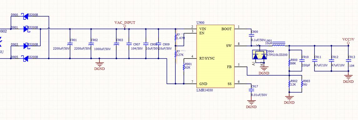
Other Parts Discussed in Thread: LMR14030

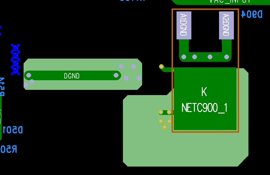
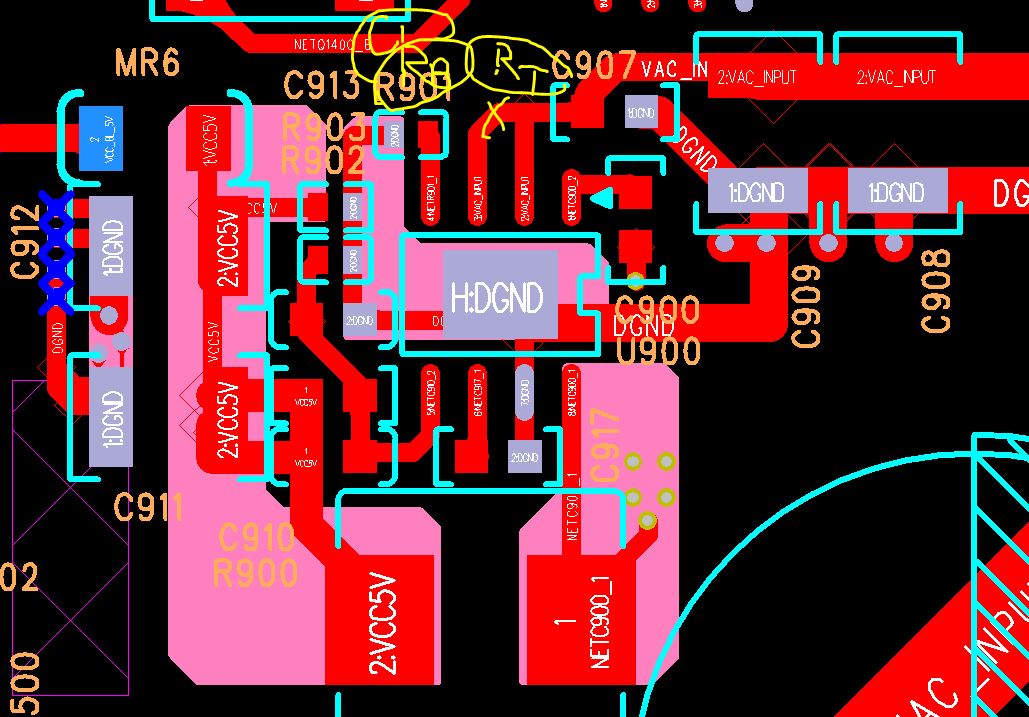
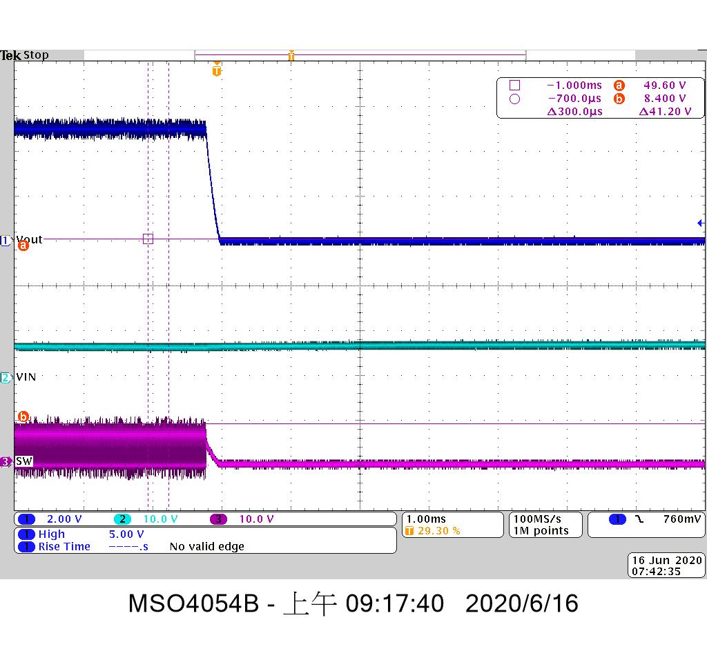
We found that the output voltage is abnormal during power off when LMR16030 is used. however, when p2p device of the LMR14030 is used, there is no problem during power off. Could you help to check if there is something missing on schematic! Especially, please check if the divider resistor for the EN pin control is ok or not?

Remark: In the customer design, there is a large capacitance of the 5500uF for the input ripple of the Full-waveform rectifier.   

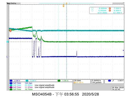
Condition: Vin:24V, Vout:5V, Iout:1.5A

***The schematic is following up the WEBENCH design. 

1. Test Result with LMR16030: CH1 VOUT 5V, CH2 VIN 24V, CH4 Input Current

2. CH1 VOUT 5V (LMR14030)

  • Hello Brian,

    Are you performing this experiment on Custom PCB or TI's EVM?

    Best Regards,

    Ankit Gupta

  • The waveforms I attached were measured on the customer board, not on EVM.

    BTW, We found a bit difference is On the UVLO threshold for both devices, is this a reason to lead to the problem. Pls let let us know what else information you need to address this issue! Pls help on this issue . Thanks!

  • Hi, 

    We tried to add one more capacitor of 0.1uF connected to low side of the divider resistors for EN pin. the problem is gone, please find the test results.

    However, please help on below questions.  

    1. Why 0.1uF can help to solve the issue?

    2. Why there is a ripple on EN pin when 0.1uF is removed?

    3. What's the side effect with the added 0.1uF.

    LMR16030 issue.pdf

    Regards

    Brian W

  • Hello Brian,

    Can you please share your layout for review. Thanks!

    -Ankit

  • Hi

    i'm the customer Brian mentioned.

    i'm not sure the pictures are inserted correctly so that i attached it again.

  • Hello Albert, Brian,

    I reviewed the schematic and layout.

    And I have a few critical points to mention after review:

    1. I don't see the high-frequency input caps of 0.47uF or 0.1uF at the input pin. I strongly recommend having these input caps for reducing the switching power loop area and for filtering high-frequency noise at inputs.

    2. You can remove one 10uF cap C907 and have one high-frequency cap instead. And please place this cap as close as possible to the IC pin.

    3. Important: I don't see the EN resistor ladder populated in the layout. It looks like VIN and EN shorted.

    4. Both FB resistors should be placed close to FB pin, it is a high impedance node and susceptible to noise.

    I believe after executing the above recommendations, you should see the issue get resolved. Right now the way layout is designed, it is susceptible to high-frequency noise and can cause high spikes on EN pin.

    I hope this helps!

    Best Regards,

    Ankit Gupta

    Application Engineer

  • 1. I don't see the high-frequency input caps of 0.47uF or 0.1uF at the input pin. I strongly recommend having these input caps for reducing the switching power loop area and for filtering high-frequency noise at inputs.

    Reply: There is a 0.1uF close to input pin in origin layout as C907.

    2. You can remove one 10uF cap C907 and have one high-frequency cap instead. And please place this cap as close as possible to the IC pin.

    Reply: As the relay1. should i still remove 1 pcs 10uF?

    3. Important: I don't see the EN resistor ladder populated in the layout. It looks like VIN and EN shorted.

    Reply: i've cut the path between pin2 and pin3, and put the RT(1.47M) and RB(127K) on the pcb, connect the point between RT/RB to EN pin for set the Start/Stop point (reffered the picture below) as the schematic Brian mentioned previously.

    but the output still abnormal with load 1.5A until i put a 100pF parallel with RB.

    4. Both FB resistors should be placed close to FB pin, it is a high impedance node and susceptible to noise.

    Reply: is it closed enough if i rotate R902 to be vertical like the second picture?

  • Hi

    let me test our EVM , and give your reply later. 

    can you help also check SS and SW voltage with and without 0.1uF EN capacitor?

    Thanks

    Daniel Li

  • Hi Daniel

    All of picture are measured in LOAD at 2A and doing power on/off

    without 100pF at ENpin as shown below

    the channel definition in picture below are:

    CH1: 5Vout

    CH2: 24Vin

    CH3: SW or SS (as shown in picture )

    Power on/off waveform with 100pF at ENpin as shown below

  • Hi Albert:

    i send a email to Brian, we can discuss this issue in email

  • ok, we'll follow up the thread in the email. and any problem will come back to you guys. thanks.