This thread has been locked.

If you have a related question, please click the "Ask a related question" button in the top right corner. The newly created question will be automatically linked to this question.

LM5060: output voltage negative workaround

Part Number: LM5060

Hi,

my customer is using LM5060 to drive a high side switch to connect/disconnect the power source to a load(resistor).

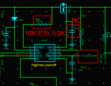
The resistor below highlilghted is 10k not 3k. Timer is left floating.

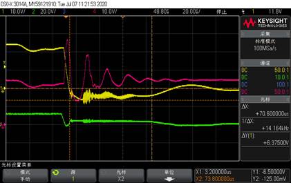
Vout is connected to the resistor load through 2m cable, when we turn off the MOSFETs at overcurrent condition, the waveform is as below:

yellow- Vout to GND, purple- Vin to GND, green- GATE to GND.

We can see that there is negative voltage appearing on Vout(-4V max), we guess it's caused by the long cable that add inductance to the load.

-4V exceeds the absolutely maximum voltage rating in datasheet. How could we solve such problem?

  • Hi Howard,

     A Schottky diode between OUT to GND helps to clamp the –ve going voltages generated due to inductive kick-back during turn-off.

    The selected schottky diode should have

    • A DC blocking  voltage rating much higher than the Vinmax
    • Non-repetitive peak surge current rating > over current threshold of the solution

     Best Regards, Rakesh

  • Rakesh,

    after circuit optimization of adding schottky diode, now the negative voltage on Vout pin is -550mV which last 66us.

    In fact, the customer has used without schottky diode for long and the device is not broken.

    In datasheet page 29

    Case D for situations where VOUT < VIN, while VOUT is negative and VIN is positive (see Figure 44). RO needs to be selected to protect the OUT pin from currents exceeding 25 mA.

    1. My understanding is as long as the current doesn't exceeds 25mA, and VOUT>-25V, the device could handle it. Is it correct?

    2. My customer is not using the Vds fault comparator to do overcurrent protection, this device is only acting as a high side gate driver, so is it okay to disconnect OUT pin with source side of the external MOSFETs? Then we don't have to worry about the negative voltage.

  • Hi Howard,

    1. Correct. Check how much current -550mV drives into OUT pin. For extra safety, I suggest to add 1k as Ro in the OUT pin path

    2. For proper drive operation and Vgs protection, OUT pin should be connected to the source of external MOSFET.

    Best Regards, Rakesh