This thread has been locked.

If you have a related question, please click the "Ask a related question" button in the top right corner. The newly created question will be automatically linked to this question.

TPS548B22: Switch frequency changed

Part Number: TPS548B22

Hi Team,

  My customer used TPS548B22 for 3.8V to 2.8V@25A buck converter application, and reported an switch frequency changed issue, could you kindly give comments on below items?

  -- In typical usage, the frequency should be fixed,  in which situation the switch frequency could be changed?

  -- How to avoid this issue?


  • Hi Benjamin,

        It is possible that the device is operating in SKIP mode. Can you please check what is the load at this condition? Also, what is the output capacitance of this application. If Cout is too little, this could cause a lot of ripple at the output. I am attaching an excel calculator that you can use to cross verify your design as well.

    Regards,

    Gerold

    TPS549B22_TPS549D22_TPS548B22_TPS548D22_Calculator_Checklist.xlsx

  • What this waveform is showing is Constant On-time "Bursting"  with a burst of 6 Constant On-times separated by the minimum OFF-time, followed by a single longer off-time to maintain regulation.  This can be caused by a couple of different effects.

    1) Low injected ramp / output capacitance

    The frequency of the Constant On-time control schemes like D-CAP3 is maintained by the output voltage charging during the ON-time and falling during the off-time.  To achieve that, there needs to be sufficient RAMP from the internal injection plus the ESR of the output capacitance to force the output voltage to rise more than it fell during the off-time.

    The internal ramp is set, along with the switching frequency, but the resistor divider on the FSEL pin.  The ramp amplitude is selected by the ramp "R" between 3xR, 2xR, 1xR, and R/2.  The smaller the resistance used to build the ramp, the larger the ramp.  Selecting the FSEL resistors with a lower "R" resistance than currently would increase the ramp and increase the frequency stability at the sacrifice of slower transient performance.

    2) Propagation Delay from Switch-node to Output Voltage Sense

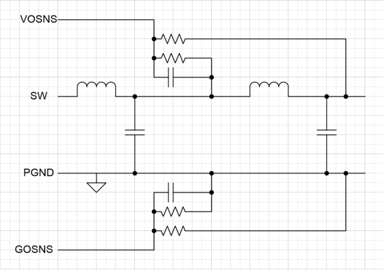
    Like an insufficient ramp (1) if there is a long propagation delay between the voltage generated at the switching node, and the output of the inductor, and the sensed output voltage, the energy delivered during an on-time may not be reflected at the sensed output voltage, so a new on-time is generated until the output voltage rises back up.  This is most often caused by power-path parasitic inductance and remote-sense capacitance at the load, or a secondary L-C filter at the output of the converter and before the remote sense.

    In this case, it can be helpful to add a capacitor from the output terminal of the inductor into the remote sense feedback to overcome the power-path delay at high frequencies while maintaining high DC accuracy with the remote sense.

    In the graphic below, the second inductance can be a real inductor, or the parasitic inductance of the routing of the power-path.

    If you can share your schematic, or at least the resistors connected to the FSEL pin, I can help you with this issue.

  •  

    It has been about 3 weeks.  If your issue has been resolved, then I will close the thread.

    If you have additional responses, you can reopen the thread by adding another post to it.