This thread has been locked.

If you have a related question, please click the "Ask a related question" button in the top right corner. The newly created question will be automatically linked to this question.

TPS40210: Tina Model

Guru 54568 points
Part Number: TPS40210

Hello,

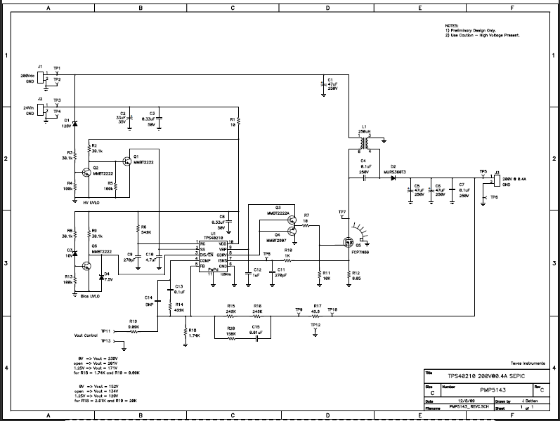
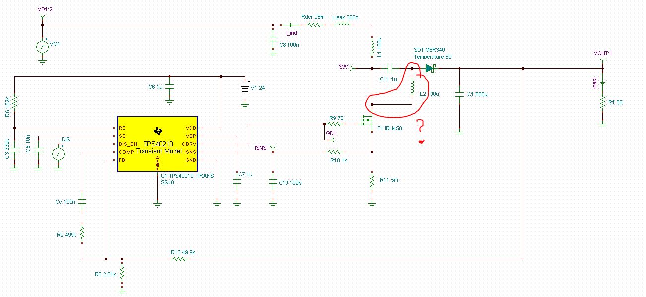
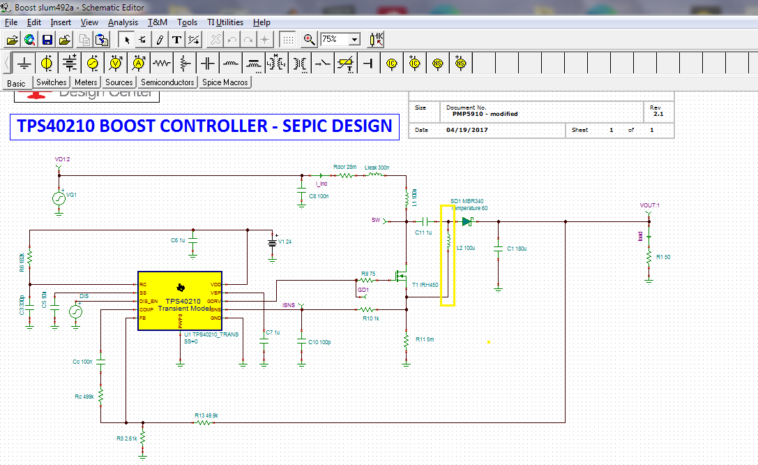
Attempting to develop SEPIC boost regulator Tina simulation via slum942a.tsc or tps40210_Trans.tsm downloads but there is no gate drive signal PWM being plotted. Web Bench also will not begin to build a circuit where +24v VDD is isolated from the NFET drain supply >170v. The NFET sources near ground so there should be no need for external Qg boost driver or switched Totem pole for isolation reasons.

Should it be possible to simulate various boost configurations with GDRV  PWM transient analysis output being plotted? Oddly Power Bench SEPIC model predicts the NFET drain voltage reaches 410v and that is also very low. All working voltages on discrete devices (SD1, C2 etc) were raised to or above VG1 and or changed to various capacitance C2 (10n-680u) produced same nonsense plots oscillator RC 150Hz-300Hz 

Thanks

Coupled T1:

  • Tina analysis only produces GDRV signal (PWM) with coupled transformer (L1 below) and crashes/locks Tina if the value of C4 >10nF/0.01uF. Also The value of SD1 parameters is very critical to stop convergence failures testing Infineon IDP30E120 1.2KVRM datasheet values entered MBR340. Oddly Tina has no basic HV Schottky diodes or NFET SPICE devices.

    Oddly if R15 R16 are >49.9k per Tina SEPIC model R13 (above post) with coupled transformer, thus GDRV output remains high during transient analysis may even crashes/locks Tina.

  • Hi Gl,

    Thank you for posting.  Please attach your TINA model file and we can run it in order to debug.   By the way, the ac coupling capacitor of 10nF appears to be too small.  It is usually in uF range.  

    Thanks,

    Youhao Xi, Applications Engineering

  • Hello Youhao,

    Thanks for the reply.

    Oddly it allowed 100nF after made inductor back to coupled and stopped crashing after that with single decoupled inductors.  Yet the gate drive PWM is not what I would expect in transient analysis plots no matter how is was configured, there is very little to no oscillator action. The model does not produce boosted output voltage above VG1 if the load is >8 amps as I recall from a week ago. The sinewave plotted output is even odder. Power Bench shows the SEPIC output to NFET source but it will only plot results from the Drain in this model like it had coupled inductors. Try RC values 150-330Kz but like Power Bench results for 880kHz. Oddly that is very low 1.5Mhz is more common for buck regulators with internal NFET. 

    Bigger problem is find coupled Toroid 50uH/100uH, 15A/20A are easy to find but no coupled Toroid or transformer in same amperage. Seemingly can make a coupled Toroid transformer by stacking two on top of each other.  

    /cfs-file/__key/communityserver-discussions-components-files/196/Boost-slum492a-.zip

  • HI Gl,

    We will take a look and get back to you within this week.  

    Thanks,

    Youhao

  • Hi Gl,

    Sorry for the delay.  I opened up your attached model file, and it is not a boost nor a sepic.  Are you sure you sent me the right TINA model file?

    Anyway, I have made some modifications but somehow the model still does not behave as expected.  This may take us a little more time than I originally estimated.

    By the way, for 160Vin and 14Vout, the sepic duty cycle is just 8%, which does not appear to be a preferred operating condition.  I think a non-isolated flyback may be more appropriate for this application, because the transformer turns ratio can help result in a proper duty cycle to operate with.  Could you consider the non-isolated flyback?

    Thanks,

    Youhao

  • Just found the attached screen shot of the original TINA schematic was corrupted. Let me attached again:

    Thanksl,

    Youhao

  •  Sorry, another try.  Hope this time it works.

    Thanks,

    Youhao

  • Hi Youhao,

    So TPS40210 Spice model did not produce PWM gate drive signal when connected any other way. Will try again but even one side L2 going to ground as if part of coupled transformer of original transient model. Yet Power Bench shows SEPIC inductor goes to NFET source but TPS40210 did not produce any PWM gate drive when connected that way.

  • The Tina transient model seems rigged to produce specific results as T1 L2 must be coupled. That is in defiance of Power Bench designs (yellow box) show similar configuration and should work with two single Toroid transformers. Note the link of ebay model in other post stacks (couples) two Toroid rings and seems very custom design. Point is the Tina model only works with couple transformer (L2 1st post) and plotted PWM gate drive (GD1) is cheesy looking at best. 

  • Hi Gl,

    I am asking  our colleague to investigate the mode issue, and get back to you,

    Thanks,

    Youhao

  • Great and it seems the TPS40210 is not behaving very well except with the original locked passive components most of which are no longer in this analysis.

    Notice the R11 when changed to 5mohm the output voltage rises a bit higher before inrush currents seems to shut down gate drive. Notice the Spice controlling inductors couple L1+L2.

  • Hi Gl,

    L2 cannot be connected to R11, because it can affect the current sense.  R11 is supposed to see the MOSFET current only.

    Our team is still investing the model, and it may take us some more time.  Will keep you posted.

    Thanks,

    Youhao

  • Hi Youhao,

    Youhao Xi said:
    R11 is supposed to see the MOSFET current only.

    So Power Bench SEPIC design will not work with TPS40210 as it seems to cause transient analysis problems. Discovered Tina transformer icon misleads as it has selection coupled inductor in same shape as transformer, not just box transformers. Gdrive is more proper looking but produces 6 amps peak (sine wave) under load or the output voltage drops to 0v if C1>20uF. Output produce sine wave due to C1=20uF, any larger value the output drops to 0V. So it seems the TPS40210 Spice model may have underlying issues. 

    Thanks for the quick feed back

  • Hello GI,

    What do you mean with "Power Bench SEPIC design"? If you are talking about the SEPIC design in Webench, it does not connect L2 to the sense resistor, it connects it directly to GND.

    I am sorry, but I do not understand your comment on transformers.

    You need to change the connection of L2, otherwise I do not expect the model to work properly. This case is for sure not modelled correctly as we do not recommend such a connection.

    I am checking the model but will need some more time for this.

  • Hi Brigitte,

    Brigitte said:
    What do you mean with "Power Bench SEPIC design"?

    Funny don't know why was saying power Bench but likely since Web Bench was part of the issue first being reported. 

    Brigitte said:
    This case is for sure not modeled correctly as we do not recommend such a connection.

    The first posted model should produce a DC output, not sinusoidal waveform. Was attempting transient results using power stage designer with TPS40210 Tina model and hit a brick wall. If C0 below is made >20uF in C1 Tina model the output is 0V otherwise pure sine wave. 

  • Hello GI,

    The model seems to have some issues that I could not solve until now.

    Would it make sense for the moment to leave the model aside and discuss the basic question you want to solve with the model?

    You want to create a SEPIC converter for 200V to 12V, is my understanding here correct?

  • Hi Brigitte,

    Brigitte said:
    You want to create a SEPIC converter for 200V to 12V, is my understanding here correct?

    Actually like to maintain ≤180vdc and current boost as the line voltage sags 8A load, unregulated 230v. Power Stage Designer above post shows us switching the NFET at 800Khz should give us that range. Power correction for isolation transformer on the AC line now sags 28-32V near 8-10A load. The input DC can be adjusted to 245v peak if needed but like to stay below 200v on the output for now. 

    Currently the unregulated DC is roughly 175v and sags to 143-146v loaded. Depending on the AC line voltage on any particular day it can vary ≤5VAC or more. Seemingly synonymous with solar panel output DC due to variance in solar radiation at any given time.

    Thanks for checking the model.

  • Set analysis to Gear 3-4 integration order then gate drive PWM indicates 1.6us (600Khz). Very high voltage in the inductor but only via very low value C11, C12 capacitors. Yet 5 amp peak load current from inductive EMF seems possible.


  • Hello GI,

    Thank you for the feedback. I do not have a good understanding of the input and output parameters you SEPIC converter shall support.

    Your model seem to work better, but as mentioned, I wonder if it makes sense for the moment to go on with the model or better just take your input and output parameters and check if TPS40210 should be able to support it or not.

  • Hi Brigite,

    According to the datasheet header SEPIC designs are supported by TPS40210. So Power Stage Designer SEPIC circuit should be possible to simulate via Tina transient analysis. The output gate drive of TPS40210 can be externally driven for greater NFET Qg and was done by TI engineer for 200v output 400mA. We have to trust Power Stage Designer tool is producing results that are possible or the tool has some issues. 

    BTW some of the issues were with the simulated diode parameters and choose another from the list.

    I'd lay odds the real TPS40210 behaves totally different than Tina model is showing. 

    Thanks for checking out things