[reposted because the images did not show correctly]
I am building a High voltage 3 Phase BLDC motor drive, operating to at 150V (Max 200V). I am using the IPB60R040 mosfets on the inverter and ISO5852S for the gate drivers. I have 3 isolated DCDC converters that supplies the high side gate drivers with 15 volts above the switch point voltage. The inverter Circuit diagram and one of the gate drive circuits are below.
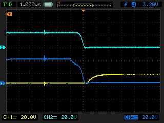
The board is working in general but I am seeing something that I don't understand and causes problems on the motor. I have to show a few scope plots to explain. The colors in the scope plots corresponds to the measurement points shown with colored arrows in the inverter circuit diagram above. Light blue is the switch node, purple is the high side switch gate and yellow is the low side switch gate. My ground reference point is at the "0Vbus". When looking at the switch node of one of the phases (blue arrow), under normal working conditions it is expected that the voltage at that point is equal to the bus voltage when the high side switch is on and low side switch off. When the high side switch starts turning off, the switch node voltage will stay at the bus voltage until the low side switch turns on (after the dead time, 1.5us in this case) the switch node voltage will drop to zero. See figure below.
(Side notes: The dead time is very long, I know, this is to better display what is happening. Also, I have some voltage spikes and ringing problems that I need to deal with as well, mostly due to parasitic inductances on a bad layout, I think. But the problem that I want to deal with here is something else.)
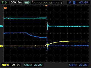
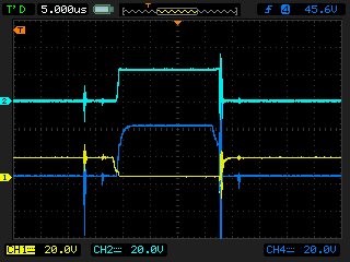
The figure above is what I see on one of the inverter phases, lets say this is phase A, which is as expected. Now, what I see on another phase/leg (phase C) of the inverter is what I do not understand. I seems that the switch node voltage drops down to zero before the low side switch turns on. See figure below.
It is as if the switch node voltage drains away before the low side switch turns on. This only happens on one of the inverter phases/legs (phase C) and only when the motor is connected to the drive. When the motor is disconnected, all the phases looks like the first scope plot figure (phase A). I has the fortunate side effect that it eliminates all voltage spike and ringing on phase C, but I don't think that this is supposed to happen, or is it? And it causes the motor to start jittering and even change direction when I ramp up the voltage to about 50V. I suspect that it is because power is lost in that phase due to this problem?
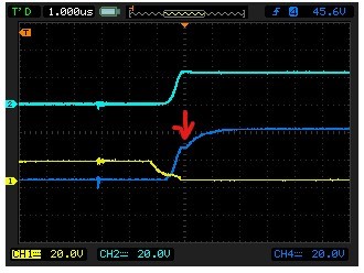
Further more, on phase B I see something similar but now it is on the turning on of the high side switch and turning off of the low side switch. What I expect is what I see in the figure below on phase C. The switch node voltage will rise only when the high side switch turns on after the dead time.
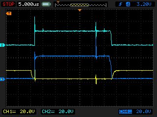
However, what I see on phase B is in the figure below. The switch node voltage rises before the high side switch turns on (which is at the mid point, red arrow, in the scope plot below). And the low side switch gate does not go down to zero
I guess this is probably because the reference point to which I am measuring (0Vbus) is moving as the low side switch turns off, causing a voltage over the low side switch drain/source, which makes sense. But why do I not see this on phase C during turn on of high side and turn off of low side? One thing that I suspected was that the low side mosfet on phase C was perhaps damaged and does not turn off properly for some reason, but I have replaced it and still get the same results. I don't really understand what I am seeing here and I am asking for some insight, maybe I am missing something?
Here are the scope plots of all three phases during switch on and switch off.
Phase A: Phase B: Phase C:
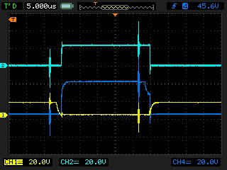
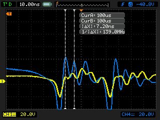
Also, I the ringing is quite bad, and I need to deal with that. It has caused some gate drivers to get damaged or at best give false/premature DESAT faults. Ideally I need to redo the layout, but for now I need to modify it to get it working. I have played around with larger gate resistance, external Schottky drain to source diodes and snubbers circuits. However, at higher voltages (100V to 150V) I still get quite some voltage spikes, especially during the low side switch on. Currently my gate resistors are 43ohm (on and off), which I think is quite large already and I am starting to compromise on efficiency. The turn on time of the low side switch is almost 2us, and yet I still see that large negative voltage spike, such as seen on phase B figure. Can I really go even slower switch time? I have tried a few RC snubber design methods, such as the app note (www.ti.com/.../slpa010.pdf) but it does not seem to work as effective. I had the best results by simply trying different capacitor and resistor combinations that I had lying around experimentally. 3.3nF and 1.3ohm has seem to help a bit. The ringing is in the high Mhz range and it seems to have a lower frequency component as well. See figure below:
Any help would be appreciated.
Thanks


