This thread has been locked.

If you have a related question, please click the "Ask a related question" button in the top right corner. The newly created question will be automatically linked to this question.

UCC256403: pin LL/SS setting and LO gate pulse during charge boot stage

Part Number: UCC256403
Other Parts Discussed in Thread: UCC25640

Hello,

I have a few questions about the pin LL/SS setting and LO gate pulse during charge boot stage.

1. Will the SS initial voltage setting still be valid when ZCS event is triggered?

2. As I read through 03/2020 revision datasheet on BMTH setting by LL/SS pin on page 38, a few descriptions confuse me. I can't find the RLL in block diagram neither on page 38 nor page 18. In the description copied below, is Rfb a typo? should Rfb be RLL?

3. It looks like before converter startup, the LO gate signal will be high for about 265us to charge boot cap, then soft startup initiates. This means split resonant cap topology can't be used with the controller, right?

Thanks.

  • previous post doesn't show a screen capture. Insert the picture again

  • Hi Sam,

    1)SS initial voltage is still Valid when ZCS event is triggered. The voltage on SS pin will be still higher than SS pin initial voltage when a zcs triggered.

    2)Yes, here Rfb should be RLL, sorry about the mistake. RLL is a resistor at 98kohm typical value in the IC and during LL/SS pin sinking the current, the sinking current will flow through the RLL to get the BMTH threshold.

    3) 265us Charging boot cap do not influence the sampling of resonant cap, so split resonant cap can also be used with this controller. Actually the controller's EVM use split resonant cap LLC. Below is a link to the EVM.

    www.ti.com/.../sluubx3b.pdf

  • Hi David,

    Thanks for your reply. I am now clear about LL/SS setting. But I am still concerned about the impact of 265us LO gate pulse on a split Cr topology. During the 265us boot charge stage, Lr and two split Cr have a free resonance which creates stress on components in the power train. In simulation, the current pulse is a few times larger than normal operation. For repeated power up/down in the field during the unit lifetime, this is a reliability concern which I prefer not to take any risk. So I will choose single Cr topology for this controller unless there is a way to disable the 265us LO high pulse. 

    Bests,

    Sam

  • Hi Sam,

    unfortunately there is no way to disable the 265us boot charge time.

    My understanding is during the start up before we have Ho pulse, there should not free resonance at split cap topology.

    are you doing the simulation using TI's simulation from the website?

    can you send the comparison waveform between split cap and single Cr during the start up?

  • Hi David,

    The resonance during 265us boot charge stage is due to the initial voltage on the split Cr, which is 0.5*Vin. The resonance starts when lower mosfet is turned on for 265us by the LO gate pulse. The free resonance will die down after a few cycles. During that brief period the current stress is high. Below is the waveform in LTspice. For single Cr topology, the initial Cr voltage is zero. LO pulse of 265us won't cause free resonance. 

  • Hi Sam,

    Before the LLC starts up, the voltage at the mid point of a split structure Cr is close to 0V, not 0.5*Vin. Yes, the split Cr structure does look like a capacitor divider but this only works as a divider for AC voltage, not DC. The PFC bus is a DC voltage with a relatively small AC ripple component.

    After switching begins, yes the DC component of the resonant capacitor voltage will be 0.5Vin but before switching begins, the voltage at the midpoint of the split CR structure will be close to 0V. This high current stress scenario is not going to happen unless you have some external circuit pre-charging the resonant cap to 0.5Vin

    Best Regards, 

    Ben Lough

  • Hi Ben,

    I run another simulation. The Vin is ramped up from 0V to 380V. The mid Cr point follows the trajectory of 0.5*vin by itself. No precharge circuit is applied. Waveform is below. It is how serial caps work. They share voltage during any time transience no matter it's dc or ac. Unless the lower cap has some leakage current path, the initial mid point voltage would be 0.5*Vin. It is one of the merits of spilt Cr topology, that the circuit can start with an initial 0.5*Vin Cr voltage.

  • Hi Sam,

    It is correct there is a resonant phenomenon the moment we have LO pulse. The resonant frequency is the resonant frequency of LLC.  The amplititue of the resonant current or voltage is related to the original votlage on the Middle point of split cap. And the highest voltage on the split cap during LO high is 0.5*Vin. Two more things you may need to consider during the simulation.

    1. The moment between we have VIN_400V and LO turns on.There is a discharge process of the split cap voltage because the resistance of low side split cap is always lower than high side split cap, that is because in UCC25640*, there are VCR cap divider on VCR pin, and RC on Isens pin, also we have low side mosfet Coss. So the voltage on the middle point of the split cap will be become lower than 0.5*Vin. There are leakage current especial through low side mosfet at this moment, so the votlage will further discharged. The discharge time depends on how fast LLC controller go through VCC start up threshold and meet the requirement of having pulses.
    2. suppose we have a voltage on middle point of split cap, then resonant phenomen happens. During the resonant process, you need to add the impedence of the resoant cap/resonant inductor/transfor into consideration. For a real case, the resonant current is very low compare to normal working condition of LLC.
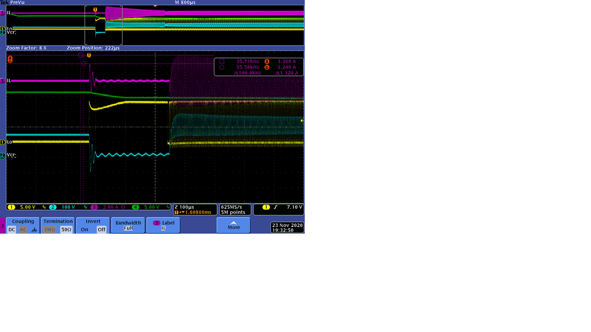
    3. I add two waveforms for your reference. the moment we have Lo pulse, middle point of split cap voltage is at about 135V. Then the current is only 2.4A, and the start up current of LLC is 3.3A. The waveform are captured using UCC25640*evm. So my suggestion is you can use UCC25640 for split cap LLC.
    4.