This thread has been locked.

If you have a related question, please click the "Ask a related question" button in the top right corner. The newly created question will be automatically linked to this question.

[UCC2720x]How to achieve the 100% duty in possible without external additional circuitry

Hi,

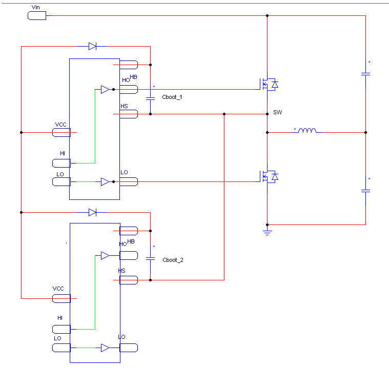
I am considering that it is used as a gate driver of Boost circuit UCC2720x.

It I will boost from 12V to 48V synchronous boost circuit . Inductor current is a maximum of approximately 100A.

I know that  it can not drive at 100% duty gate of the high side to charge the bootstrap condenser.

Can I achieve a 100% duty by an external circuit? 

Or Is there automotive products its absolute maximum voltage is over 100V  and can drive 100% duty?

Because I'm very hurry, please tell me  any information.

Thanks.

  • At 100% duty cycle the bootstrap capacitor will eventually discharge to the point where the HO output can no longer keep the high side MOSFET turned on.

    If you need to operate at 100% then you will have to generate a separate bias rail for the bootstrap capacitor

    Alternatively - and this is just a suggestion. You could have two driver devices each running at a maximum of 50% duty cycle at 180degrees out of phase. Or have two drivers, use one to generate duty cycles from 0 to 50% and the other to generate only the additional duty cycle over and above the 50% generated by the first driver. ie, for a 25% duty cycle, driver 1 operates at 25%, driver 2 operates at 0%. For a 66% duty cycle, driver 1 operates at 50% duty cycle and driver 2 operates at 16% duty cycle - of course driver 2 output should go high as driver 1 reaches the 50% point.

    There are ways to generate a 100% duty cycle using a gate drive transformer - Basically, you need to generate a 'carrier signal' lets say 200kHz, 12V square wave. This can pass through a gate drive transformer where it is rectified on the secondary . By turning the carrier signal on and off at what ever switching rate and duty cycle you need, you can turn the SRs on and off. This would work best at lower switching frequency rates - say up to 50kHz or so.

    Regards
    Colin
  • Hi Colin,


    Thank you for your reply.

    Is there no way to charge from outside the bootstrap capacitor?

    If it can be achieved with an external circuit method is simple above,  I think it can be cheaper than the IC use two.

    Whether this method would be difficult?

    Please tell me if there is advice.


    Thnaks

    Tomoaki Yoshida.

  • Hello Tomoaki-san

    The problem is that the idea I suggested above, with two gate drive ICs, won't actually work !. Apologies for this.

    Anyhow, there is more than one way to tackle this problem. You can keep the bootstrap capacitor charged by using a small high frequency transformer to generate the 12V rail for the Bootstrap capacitor. This allows the driver to keep the top side MOSFET ON for as long as  you like.

    the transformer requirements are pretty simple - drive its primary from a 12V supply and rectify the output. You may have to put some small resistive load or a zener diode on the output to keep the HB output within reasonable limits. You could find a suitable transformer if you look for gate driver transformers on the web.

    Of course you could use the rectified transformer output to drive the MOSFET directly. This would require that you can generate a carrier signal (VSQ above) and be able to turn it on and off using the HI signal. Àll in all it may be simpler to use the arrangement I suggest above.

    Regards

    Colin

  • Hi Colin

    Thank you for your reply.

    Why two gate drive ICs won't work?
    I thought it's good way.
    Please tell me reason it does not work.

    I would have asked to send in a circuit diagram of you, I was not able to see it.
    Could you send it again?
    Since I do not make much this way.

    Thanks

    Tomoaki Yoshida.
  • Hello Yoshida-san

    The reason it won't work is that - if you have a 100% duty cycle provided from two high side gate drive ICs then the switched node (SW in the diagram) will always be at or close to Vin. This means that the diodes which are used to charge the bootstrap capacitors (Cboot_1 adn Cboot_2) are always reverse biased an the bootstrap capacitors will eventually discharge below the UVLO point of the driver. Essentially, with this arrangement there is no way to replenish the charge in the bootstrap capacitors. This is why it won't work and to be honest I should have thought of that before posting. I tried to think of ways to overcome this problem but I didn't find it. The transformer / gate driver solution I posted earlier will definitely work.


    Regards

    Colin