This thread has been locked.
If you have a related question, please click the "Ask a related question" button in the top right corner. The newly created question will be automatically linked to this question.
Hi,
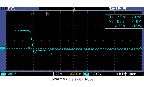
We use the LM3671MF-3.3 in a design that has shipped around 2000 units. I have recently had three boards fail with the output of the LM3671MF-3.3 a low resistance (0.5 to 3 ohms). After swapping just this part the board is functional again.
Prior to swapping I checked for solder joint issues or visible damage elsewhere. To be sure I reflowed the joints and retested but in this case the output seems shorted and the power supply does not start up despite 5V on the input.
In this design I have enable tied to VIN which I found is not recommended (I have another post asking about the risks of this). However I have performed full load step tests, power on/off tests, steady full load tests and current limit tests and the part seems to maintain regulation and function within expected limits.
As this is a synchronous design I am wondering if this could be a failure of the rectifier FET.
I wondered if anyone could possibly provide some insight into what could cause the switch node to be near short circuit to 0V.
I had a thought about whether there was a chance the 3.3V switch node could be powered while the input 5V supply was off but I cannot see this in measurement or studying the design. Is it worth adding a diode from output to input (I guess the internal PFET has one) in such designs to make sure power on the output bypasses the device?
Thanks in advance, Mark
Thank you for your reply.
I have been reading up on failure modes of smps mosfets. One thing I need to check is the switch node ringing level to make sure the low side synchronous fet is not being over stressed.
I may need to add a snubber circuit to dampen this. The layout is very tight with wide traces and all components close to the IC so little more I can do to reduce parasitics.
I have added a voltage detector to set enable high only when vin is greater than 3.0V. I was worried that enabling the part below its minimum voltage may cause shoot through damaging the low side fed.
Hi Sheng,
To me that sounds more like the fact that exceeding VIN+0.2V would forward bias the diode in the high-side switch?
Surely being a synchronous converter there will inevitably be some ringing at the switch node in any design.
Does the internal synchronous N-FET have an absolute voltage breakdown to know what to limit that ringing to in order to be safe?
For reference the switch node waveforms are shown below. The ringing does exceed VIN+0.2V - I am sure this won't be the EOS level of the FET (why only design in 0.2V margin to breakdown?!). But I do need to know if this needs suppressing with a snubber.
Note this was measured with short ground clip but only a 200MHz bandwidth scope and 16pF probe. Always difficult to know the true ringing level when themeasurement setup could be affecting it.
Overshoot to 5.92V, undershoot down to -2.84V.
Could you let me know if this is a design risk and any recommendations for mitigation?
Mark
Any news on the maximum switch pin voltage? I can't believe the low side fet is damaged at vin+0.2V, it must have a higher breakdown.
synchronous converters are likely to have some switch node ringing caused by layout parasitics. My current layout is tight around the IC with short wide copper pour traces
I could possibly add a snubber but I would have to move the inductor and output cap further from the switch node which seems counter productive.
Thanks, mark
Ok. So what is the likely cause of the large negative spike? I appreciate I could add a snubber circuit but this would involve pushing my inductor further away from the IC to allow room for the R and C. This would add further parasitics to the layout.
I have also read about adding a low side schottky - this kind of negates the purpose of a synchronous converter if I need an additional external schottky but I am not too sure at the moment how this would help with the negative spike.
My other thoughts for review are the inductor specification to see if this is compounding the spikes seen. Of course with my 16pF scope probe attached could this be creating the spikes that are not really there with the probe removed?!
My layout is as shown below (apologies for the colour scheme!):
The grey trace is 5V coming into the converter. The green is 0V, pinky colour 3.3V. The inductor layout is quite tight.
The circuit to match above is below:
I would appreciate any advice on typical 'spike removal' techniques while I look in more detail at the design.
The PCB this is used on is currently waiting release based on this last detail so I am keen to get this resolved if possible.
Thanks, Mark
Sheng,
I do not want to change this part at this stage. We have several thousand boards in use with this part at the moment but just three recorded failures due to this IC output short circuit. I have measured the same spike on other boards and with new replacement parts.
I have recently modified the design because enable was tied to Vin and the parts appeared to have failed after powering down the board and then they would not power up again. I was concerned the enable control may have caused the failures and now have a voltage monitor to enable when VIN >2.7V.
During this investigation I have revisited the switching waveforms and noticed the spikes. There is a nice application note from Infineon called "Buck Converter: Negative Spike at Phase Node" which talks about this. A lot of application notes concentrate on the positive ringing and do not give any explanation for the negative spike.
To be sure the issue is not enhanced by my scope probe I have 'double probed' the inductor and see the same waveform on both probes with no noticeable difference in shape adding a second probe. I am therefore fairly confident that this is not created by the addition of the probe.
I am not sure whether the spike is a real risk to the internals of the converter. By adding additional components I will push out the loop to add room for the parts potentially making the spike worse. I would be really interested if you can measure this on an LM3671 development board at TI.
My layout is quite tight and I am not sure how I can improve things other than reducing the short trace inductance from the ground pin. This trace is 2mm long and 0.4mm wide so could be a fraction of a nH.
I thought about connecting the 0V pin directly to the 0V plane as you suggested but then the switching loop would have to traverse two vias to complete the circuit. The sum of the via inductance would be greater than this short trace inductance so it seemed better to go for a short trace on the top layer as all input/output caps are referenced to a mini-flood on the top layer.
As discussed an external schottky or snubber could be added at the expense of adding parasitic inductance to the loop to make room (catch22 situation?).
What would TI recommendation be?
Mark
With the additional diode the -ve excursion is clamped at a lower voltage. Presumably the step between the two vertical cursors is caused by the dead-time of the synchronous converter. I.e. primary fet turned off, signal tries to go -ve but clamped by the synchronous fet body diode until the dead time ends and the synchronous fet is enabled and the diode is 'shorted'.
Surely then the leading -ve edge is caused due to the reverse recovery of the body diode / fet capacitance unable to react ideally and preventing the signal being instantaneously clamped?
Mark
With regards to the comment:
"-2.5V negative spike is way too big and can damage the NMOS body diode"
I believe the low side mosfet (synchronous) is the NMOS part (going by the block diagram in the DS this uses a PMOS on the high side).
I am wondering how the -2.5V spike can damage the NMOS? Technically if the switch node is -2.5V relative to 0V then the forward voltage across this diode is 2.5V briefly during switching. When the diode is active it would clamp to its forward voltage so I guess this additional voltage is caused by the inductances either side of the NMOS and the resulting voltage generated by the rapid changing current. Therefore would the NMOS actually see less of a voltage (the rest being generated across the bond wire inductance for the 0V and switch node pin)?
Could you help by explaining the mechanism whereby the low side MOSFET would be damaged by this?
It is not particularly easy to model this behaviour as I do not know enough about the internal structure of the part to get a representative model. The TI-TINA model seems to be a bit 'ideal' and even with external parasitics modelled does not really create any over/undershoot.
Mark