This thread has been locked.

If you have a related question, please click the "Ask a related question" button in the top right corner. The newly created question will be automatically linked to this question.

WEBENCH® Tools/LM5122: WEBENCH does not recommand to use the LM5122 for a 9Vin to 36Vin ; 48Vout @ 3A; Dual-Phase Synchronous Boost Converter

Part Number: LM5122

Tool/software: WEBENCH® Design Tools

Hi,

I would like to design a Boost converter with the following characteristics:

Vin : 9-36V,

Vout : 48V

Iout : 3A

Switching Frequency : 500Khz.

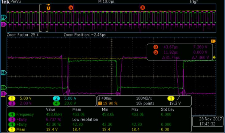
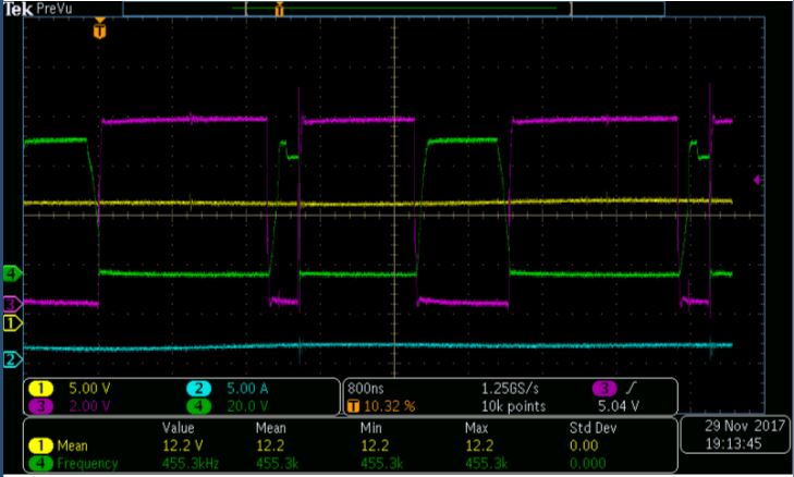
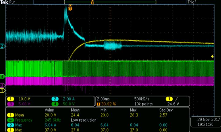
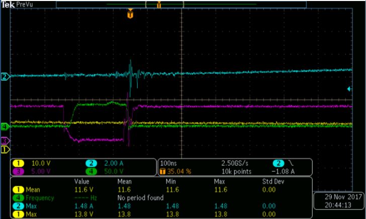
I did some tests with the LM5122EVM-2PH (Foced PWM mode), and I think that's the LM5122 is good component for my applicaiton.

I would like to define a dual phase interleaved and I need to choose the MOSFET and inductance value. But Webench designer does not recommand to use the LM5122 :

"Can't find suitable FET for the design"

image.png

I don't understand why? The PMP7965 reference design seems to be close to my design.

Thanks,

Jerome

  • Hello Jerome,

    Please be aware that WEBENCH might not be able to do a design for all possible applications. In this case WEBENCH doesn't have the functionality to implement a 2 phase design or use multiple FETs. This is most likely why the design is not able to complete.

    That being said, the LM5122 is a great choice for this application and PMP7965 is a good sating point and reference. Inductor values can be calculated using the equations found in the datasheet.

    Thanks,

    Garrett

  • Hi,

    So, i did somes tests with LM5122EVM-2PH Evaluation Module to evaluate the LM5122.
    My boost characteristics is :

    Vin = 9-36V

    Vout = 48V

    Dual Phase, Iout per phase : 1,5A(MAX)

    I replaced the following components of the eval board in order to be close to my need :

    RES = 0Ohm, R33 = 20K, R34 = 68K, R31 =20K, R29 = 20K, MODE = VCC (Forced PWM mode).

    I did not change the L1 and L2 value, I calculated 13uH. 

    I have an issue with the High-side and Low- side gate drive outputs, the LM5122 controller drives the HIGH and LOW MOSFETs in same time :
    CH1 = VIN, CH2: Input current, CH3 : LO (R5) and CH4 = HO (R6)

    Did you know why I have this issue with the MOSFET driver outputs.

    Thanks,

    Jérôme.

  • Hi Jerome,

    The signals that are being observed might not be real. Is the ground lead of the probe short? If a standard long ground lead is used this can couple noise into the probe that is not real. Please use a short ground lead to measure these signals.

    Please change the output capacitor voltage rating as well. On the 2 phase EVM the output capacitors are only rated to 35V and the output is now 48V...

    Thanks,

    Garrett
  • Hi Garett,

    I used 3 probes, and the ground leads attached to TP10, TP7 and TP8 of the eaval board.

    I did not observe this issue whit a light load, only with a high load:

    See below  the High-side and Low- side gate drive outputs with a light load (CH3 : LO (R5) and CH4 = HO (R6))

    My real issue is : there is reverse current goes to laboratory power supply (Vin) that 's increase the input level (CH1) to 37V :

    CH1 = VIN, CH2: Input current, CH3 : LO (R5) and CH4 = HO (R6)

    There are 5 x 6800uF capacitors connected to the output of the eval board. These capacitors are used like capacitors tank.

    OK, I have to change the output capacitors on the 2 phase EVM.

    Thanks,

    Jérôme.

  • Oscilloscope screenshots with SW1 signal (CH1 = VIN, CH2: SW1, CH3 : LO (R5) and CH4 = HO (R6))

  • Test with a second eval board, only stuff changed : the switching mode = Forced PWM (R22=R23=0R & R26=R28 = DNP): 

    CH1 = VIN, CH2: SW1, CH3 : LO (R5) and CH4 = HO (R6)

  • Hi Jerome,

    Looking at the waveform that you are providing still believe that this related to probing. Even though the ground leads are connected to the probe points this doesn't mean that the leads are short. Please see this blog post about how to measure high frequency signals. This will help when you are measuring the switch node wave forms. Since you are using three probes to measure these waveforms please be aware the HO is riding on the SW voltage, so HO will be about the 7V above SW when the HO switch is truly on. Also if you are seeing reverse current please try operating in diode emulation mode (MODE = GND). This will make sure that there is no reverse current in the inductor.

    There also looks to be a large amount of jitter and instability. Please make sure that you have performed the datasheet equations to make sure the component selections is correct. Since the design is considerably different that the EVM the compensation , current sense resistor and the slope resistor might need to be changed for improved operation.

    Thanks,

    Garrett

  • Hi Garett,

    About the reverse current, I tried in diode emulation, and you are right, there is no reverse current.

    I changed the resistors of slope and curent sense , the boost seems to be more stable.

    Now, I would like to compare the Skip-Cycle Mode and Pulse-Skipping Mode, I seek a boost configuration where i have less noise on the output.
    Fisrt, i had chosen the forced PWM mode, because, the switching frequency does not change. I little aware that with Pulse skipping mode, there are some harmmonics of the switching frequency on the ouput.

    Do you have applicaiton note which describe the Skip-Cycle Mode and Pulse-Skipping Mode ?
    Thanks,

    Jérôme.

  • Hi Jerome,

    Unfortunately there is no application note that describes the difference between the two mode. Here a brief summary and comparison of both the modes

    1. Pulse skipping mode: The controller will skip pulses as needed (VCOMP < COMP to PWM offset) and results in a fairly random switching pattern. This switching pattern results in low output voltage ripple.

    2. Skip cycle mode: The controller will only be on for a short period or time and continue to switch until the output voltage is slightly above the output voltage. Once this target has been achieved the controller will not switch until the output is below the specified lower value. This results in more ripple on the output voltage than pulse skipping. However the input current due to switching should be lower since there are only short periods of switching.

    In your application if you want less ripple during light load operating than I would suggest selecting pulse skipping mode.

    Thanks,

    Garrett