Part Number: AM62L
Other Parts Discussed in Thread: AM6442, AM2434, AM6412, AM6411, AM2432
Tool/software:
Hi TI Experts,
I have the below queries regarding the ADC0 peripheral
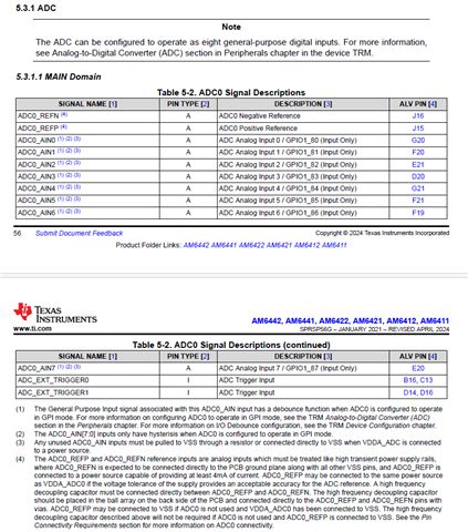
1. Supported ADC resolution and channels
2. Guidelines for using ADC peripheral
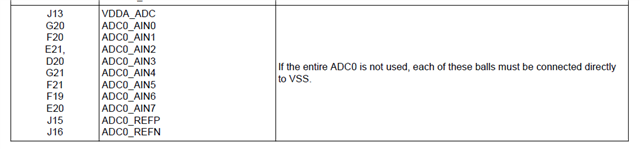
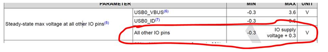
3.ADC0 input range
4.ADC inputs used as GPI
Let me know your thoughts.