This thread has been locked.

If you have a related question, please click the "Ask a related question" button in the top right corner. The newly created question will be automatically linked to this question.

AM3358: McASP rise time / fall time

Part Number: AM3358

Hi,

1) My customer is asking about below rise time / fall time requirements.


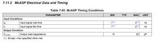
What is the percentage of the voltage level for the input signals?
Below E2E said it is between VIL and VIH. This means between 0.8V(24%) to 2V(60%) if VDDSHVx=3.3V.
https://e2e.ti.com/support/processors-group/processors/f/processors-forum/709993/am3357-mcspi-input-signal-rise-and-fall-time

On the other hand, below E2E concluded it is between 10% to 90%.
https://e2e.ti.com/support/processors-group/processors/f/processors-forum/557399/am335x-rise-fall-time-definition

Which one is correct?

2) What happens if rise or fall time is less than 1nsec?
It may lead to unexpected behavior?

3) Customer does not see such min. requirement in other devices.
Why the min. requirement is defined?

Thanks and regards,
Koichiro Tashiro

  • Hi Tashiro-san,

    If the signal transitions too fast at the AM335x input pin, it can turn on the ESD cell which can sink a lot of current. If the signal transitions too slow it can remain in the threshold region for too long causing both P- and N-regions of the CMOS input buffer to shoot through, eventually causing electromigration damage. It is best to adhere to the datasheet requirements.

    The transmission line on the PCB signal trace can take some of the edge off of fast rise and fall times. Recall a transmission line can is modeled with connected resistors, inductors, and capacitors which slow the edge rate down. The datasheet for the output buffer of the connecting device might have a rise/fall time that is faster than the Table 7-80 McASP Timing Conditions minimum timing, but the rise/fall time may be within range at the AM335x input pin. This can be measured or simulated with HyperLynx.

    If the ESD cell turns on for a signal with rise/fall that is faster than the datasheet requirement, the signal will become distorted as the ESD clamp sinks lots of current.

    I will ask what voltage levels is assumed for the rise/fall timings. Give me a couple days.

    Regards,
    Mark

  • Hi Tashiro-san,

    The minimum rise/fall time is set to a realistic minimum to bound the timing analysis exercise.

    Maximum rise/fall time (slowest) is the one that usually limits performance. We try to specify a realistic minimum to bound the timing analysis. The timing models we use in timing analysis need a bounded rise/fall time so using 0 (or infinite slope) results in inaccurate and sometimes just wrong timings.

    It seems unlikely in real world applications, that the chip would be driven so fast that the fastest input slew rate (smallest rise/fall time) would cause issues.

    To avoid the ambiguity of the voltage thresholds assumed for the rise/fall timing, datasheets of newer devices like AM64x specify a min and max input slew rate instead of a time between two voltage thresholds that are not explicitly defined.

    Hope this helps,
    Mark

  • Hi Mark,

    I am not sure I understood your reply correctly.
    Could you clarify which parameter customer needs to follow for AM335x McASP input/output slew rate?

    Thanks and regards,
    Koichiro Tashiro

  • Hi Tashiro-san,

    My apologies. For AM335x, the voltage thresholds for the tRise and tFall timings are not specified in the datasheet. The part is old and the thresholds cannot be confirmed.

    If the customer wants to be conservative, then they can assume worst case thresholds for min and max tR/tF.

    For min tR/tF, assume the 1ns is for the input signal to transition from VIL to VIH (tR) or from VIH to VIL (tF). If the connected device signal rise/fall time is specified from 20% to 80% then the transition from VIL to VIH will be faster.

    For max tR/tF, assume the 4ns is for the input signal to transition from 0% to 100% (tR) or from 100% to 0% (tF). If the connected device signal rise/fall time is specified from 20% to 80% then the transition from 0% to 100% will be slower.

    If the connected device satisfies these worst case rise/fall times then it will certainly satisfy the actual rise/fall requirements that cannot be precisely defined due to missing voltage threshold information needed to define the rise/fall times.

    Again, the rise/fall time must be satisfied at the AM335x device input pin (not at the output pin of the connected device). The board trace may smooth out the edges, slowing down the rise/fall time from the connected device. Additional components like a series resistor may be implemented to further slow the signal edge rate if necessary.

    Hope this helps,
    Mark

  • Hi Mark,

    I see. I close this item.

    Thanks and regards,
    Koichiro Tashiro

  • Hi Tashiro-san, thanks for closing this ticket!