Other Parts Discussed in Thread: TPS6594-Q1
We found TPS6594-Q1 spec said in 5.6.1:
The registers in the TPS6594-Q1 device are organized into five internal pages of 256 bytes each. The first 3 bits of the 11-bit register address offset indicates one of the following pages which the register belongs to:
• Page 0: User Registers
• Page 1: NVM Control,Configuration, and Test Registers
• Page 2: Trim Registers
• Page 3: SRAM for PFSM Registers
• Page 4: WatchDog Registers
but also said in 5.5.2:
The default I 2C1 7-bit slave device address of the TPS6594-Q1 device is set to 0x48 (0b1001000 in binary), while the two least-significant bits can be changed for alternative page selection listed under Section 5.6.1.
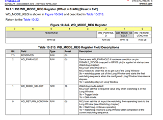
so I think if i want to set WD_MODE_REG Register in PAGE4.(offset is 0x406)
slave addr is 0x4c(0x48+4),reg addr is 0x6. Right?
root@j7-evm:~# i2cget -y -f 2 0x4c 0x6
0x20
But this register reset value is 0x2.why?