A related question is a question created from another question. When the related question is created, it will be automatically linked to the original question.
If you have a related question, please click the "Ask a related question" button in the top right corner. The newly created question will be automatically linked to this question.
Please provide more details with respect to the conditions required to create the different clock waveforms. For example, does it vary based on PCB assembly or is it completely random on a single PCB assembly?
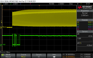
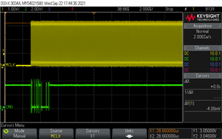
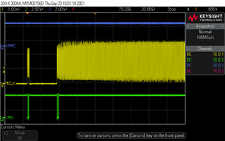
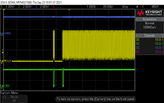
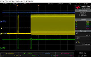
Were these scope captures taken on the same board, where the clock waveform looks good sometimes and looks bad another time? If so, this issue needs to be understood as this should not be happening. It looks like there is some contention on the signal or IO power supply when this occurs.
What components are connected to MMC0 and how many of the MMC0 signals are being connected to external components? Is the AM335x VDDSHV4 IO power rail being powered from the same power source as the attached device IO power rail?
Can they capture the AM335x VDDSHV4 IO power supply voltage on another channel when this occurs?
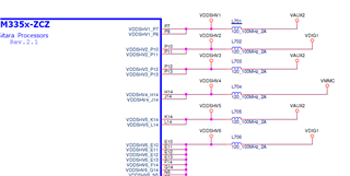
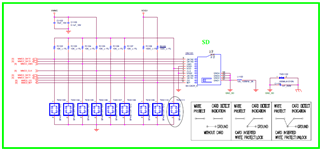
Can you include a schematic snapshot that includes all MMC0 signal connections? Also provide power supply connections to AM335x and attached device.
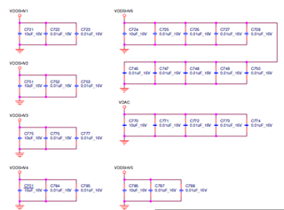
I did not see any de-coupling capacitors between on the AM335x VDDSHV4 power pin after low pass filter L704. Were these accidently omitted in the snapshots provided? If not, each power pin needs local de-coupling capacitors after their respective low pass filters.
I’m concern with the SD Card ground connections. Hopefully the SD Card VSS1 and VSS2 pins are connected directly to the same ground as the AM335x device. I assume the other grounds shown for the SD Card are simply the metal chassis ground and they are not part of the SD Card signal and power ground connections.
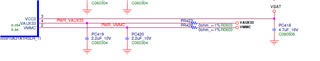
They should not be using a zero ohm resistor for R514. This should be a 22 - 50 ohm resistor. The MMC/SD host controller in AM335x loops the clock back at the pin to improve timing margin for the internal circuits. However, there is a negative side effect of implementing clock loopback on a pin. The clock signal will be distorted on the source end of a signal trace and a series resistor of 22 - 50 ohms is required to modify the signal distortion such that is does not create a glitch on the looped back clock signal.
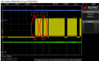
I will explain what happens. The clock output buffer inside AM335x has a source impedance of about 30- 50 ohms and a typical PCB signal trace has a characteristic impedance in the range of 40 - 60 ohms. When the output buffer toggles the signal from low to high or high to low, the voltage of the pin which sits between the output buffer and the PCB signal trace will not transition to the expected voltage immediately. This is because the output buffer impedance and trace impedance create voltage divider that causes the pin to step to a mid-supply voltage for a short time. This step will last as long as it takes for the clock signal to travel down the PCB signal trace to the SD Card, where it encounters a high impedance load that creates a reflection that allow the voltage to increase to VDD or VSS. The amplitude of the mid-supply voltage step may be near the AM335x clock buffer input switching threshold, which allows noise to create a glitch on the AM335x internal clock. The series resistor raises the impedance of the PCB portion of the voltage divider such that the voltage at the pin steps above or below the switching threshold.
I suspect this is what is causing the instability and the reduced clock amplitude is contributing to the issue.
1. Yes, we have de-coupling capacitors for AM3354 each power. Please refer to below snapshot.
2. Yes, SD Card VSS1 and VSS2 pins are connected directly to the same ground as the AM3354 device.
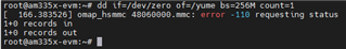
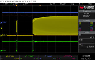
3. Per change R514 from 0 to 22 Ohm, the SD -110 error didn't happen any more, but I can't find obvious improvement from waveform.
4. We try to change TVS1106 to ultra low capacitance type (from 2.5pF to 0.35pF), the SD -110 error didn't happen any more also and the waveform have obvious improvement.
I didn't clearly understand why have 3&4 result, could you please help to explain?
Do you suggest to implement R514 (22 Ohm) and TVS1106 (0.35pF) two solutions simultaneously?
*SCH - CPU De-coupling CAP
* Waveform - Change R514 from 0 to 22 Ohm
* Waveform - Change TVS1106 form 2.5pF to 0.35pF (R514 keep 0 Ohm.)
It appears you had two problems and both need to be fixed.
The ESD protection device was clamping the signal, which caused reduced amplitude. You need to discuss this topic with the manufacture of the ESD device. None of the digital signals in your system should be clamped by the ESD device during normal operation, where it reduces signal swing.
I explained the purpose of the series resistor. A series termination resistor in the range of 22 - 50 ohms should be located as close as possible to the AM335x MMC0_CLK pin to shift the clock distortion away from the looped back clock input buffer switching threshold.
What you observe on this signal depends on where you connected the probe, the bandwidth of your probe/scope, and quality of your scope probe ground.
You will need a very high bandwidth probe and scope to observe short over-shoot, under-shoot, and non-monotonic events on the signal. I recommend using a low capacitance FET probe with a very-very short low loop inductance ground.
You will see a mid-supply step on the signal when probing near the source. This occurs because the output impedance of the MMC0_CLK output buffer, series termination resistor, and characteristic impedance of the PCB signal trace creates a voltage divider. The voltage divider output is applied to the source end of the PCB signal trace. This voltage propagates down the trace to the far end where it encounters a high impedance load which causes a in-phase reflection that returns to the source. Therefore, the voltage transition observed on the far end will be a continuous transition between VSS and VDD. The is not the case for the source end, as it steps to a mid-supply determined by the voltage divider values and the transition only continues to VDD or VSS once the reflection returns from the far end. You need to select a series resistor value that allows the MMC0_CLK pin to step through the voltage of (VDDSHV4 / 2) without pause. I suggest the step observed on the MMC0_CLK pin should be at least 200mv above (VDDSHV4 / 2) on the rising edge and at least 200mv below (VDDSHV4 / 2) on the falling edge.