This thread has been locked.

If you have a related question, please click the "Ask a related question" button in the top right corner. The newly created question will be automatically linked to this question.

Linux/AM3352: MMC clock timing

Part Number: AM3352
Other Parts Discussed in Thread: SYSCONFIG

Tool/software: Linux

Hi expert,

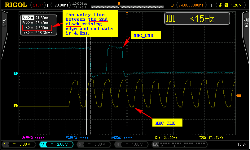
In AM3352 datasheet table 7-90, we see that in opp100 high speed mode, td(CLKL-CMD) and td(CLKL-DAT) is in 3ns - 14ns, customer measure the timming of  td(CLKL-CMD) and td(CLKL-DAT), found the real value of this parameter is different for every cmd or data.

I want to confirm that if the value of  td(CLKL-CMD) and td(CLKL-DAT) is different for every cmd and data and the scope is between 3ns - 14ns?

Thanks!

  • The factory team have been notified. They will respond here.
  • Read the following E2E post to see it it answers your question.

    http://e2e.ti.com/support/arm/sitara_arm/f/791/p/633651/2353137#2353137

    Regards,
    Paul

  • Read the following E2E post to see if it answers your question.

    http://e2e.ti.com/support/arm/sitara_arm/f/791/p/633651/2353137#2353137

    Regards,
    Paul

  • Hi ,

    It did not answer my question. You just gave another question in the end, not answer it.

    I want to know that if THE DELAY TIME is dynamic changed  for every cmd and data transmission, and the scope is between 3ns - 14ns?

  • I mentioned the previous post because there have been a few cases where someone did not get the expected result and we found it was because they were measuring the delay relative to the wrong clock edge based on their configuration of the HSPE bit.


    The delay values provided in Table 7-89 and Table 7-90 define the range of delay for each CMD and DAT output relative to the clock output. This range represents the worst case delay value across process, voltage, and temperature variations. It also includes delay variation introduced by circuit delays and propagation delays which will cause delay variation across the outputs. So you are correct, the delay is different for each output and the data sheet only defines the range of each output relative to respective clock edge.


    The delay of each output should remain fairly constant for any one device with only small changes resulting from voltage and temperature variations. I would also expect the relative delay differences from one output to another to remain fairly constant from one device to another.


    Let me know if this answers your question. If not, you may need to provide more detail the help me understand your question.


    Regards,
    Paul

  • Hi Paul,

    Thank you, I got it.

    Another question, I have set some register bits  to apply the automatic clock gating strategy:

    - SD_HCTL[2] = 1    ==>   High speed(48MHz)

    -  SD_SYSCONFIG[0] = 1, SD_SYSCTL[CEN] = 1, SD_CON[16] = 0   ==>    automatic clock gating strategy

    The measured results are shown as follows. Is the first clock invalid?? 

  • Clock transitions are used to synchronously transfer data to/from the card via CMD/DAT signals. The clock can run continuously or be stopped between transfers to save power.

    I was only able to find one requirement related to stopping the clock in the SD Card specification. It discusses a requirement to continue the clock for 8 cycles after the end bit or status token. Therefore, I assume driving the clock one cycle before the transfer begins is allowed.


    Regards,

    Paul

  • I got it, Thanks a lot.