This thread has been locked.

If you have a related question, please click the "Ask a related question" button in the top right corner. The newly created question will be automatically linked to this question.

TMS320C6747: FPGA on EMIFB interface

Part Number: TMS320C6747


Hello, Mark.

As per your previous answer, I'm trying to move the FPGA on EMIFB SDRAM interface.

However, I have some questions about the address and data bus pins connections.

As Section 19. EMIFB, SPRUH91D.pdf (TMS320C6745/C6747 DSP Technical Reference Manual (Rev. D)), 

there are 4 examples for connecting the address pins of 32bit EMIFB interface in the Table 19-4.

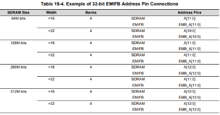
I want to use all of 256MB, which is the maximum address areas of EMIFB, but the address pins are limited to 0~12 and BA 0~1. 

I wonder if it is necessary to allocate and use additional address pins as GPIO pins like EMIFA, or if there are other methods.

Regards, 

Youngho.

  • Hi Youngho,

    See Table 6-23. EMIFB Supported SDRAM Configurations(1) in the datasheet https://www.ti.com/lit/ds/symlink/tms320c6747.pdf

    The SDRAM protocol uses two phase to latch the address.
    First it sends a ROW address. Then it sends a COL address across the same address bus.

    See also datasheet Figure 6-24. EMIFB Basic SDRAM Write Operation and Figure 6-25. EMIFB Basic SDRAM Read Operation
    The same is shown in TRM Figure 19-6. Timing Waveform for Basic SDRAM Read Operation and Figure 19-7. Timing Waveform for Basic SDRAM Write Operation. It shows ROW address is latched before COL address. https://www.ti.com/lit/ug/spruh91d/spruh91d.pdf

    EMIFB supports 8, 9, 10 or 11 column address bits
    EMIFB supports up to 13 row address bits
    EMIFB supports 1, 2 or 4 internal banks

    If you have a 32-bit data bus, then Table 6-23 shows that you should use 13 Rows (max), 11 Columns (max), and 4 Banks (max):

    2^13 * 2^11 * 4 (banks) * 4 (bytes per 32-bit data) * 1 chip select = 256 MBytes

    Your FPGA should emulate an SDRAM for the EMIFB to properly communicate. It doesn't need to respond to all of the commands exactly the same as an SDRAM. Refer to JESD21-C Standard 3.11 Synchronous Dynamic Random Access Memory (SDRAM)
    SDRAM FUNCTION TRUTH TABLE is in under section 3.11.5.1 -- General SDRAM Functions

    Perhaps there is an example out there that you can start with?

    Regards,
    Mark