This thread has been locked.
If you have a related question, please click the "Ask a related question" button in the top right corner. The newly created question will be automatically linked to this question.
Hello TI Colleagues,
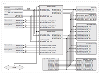
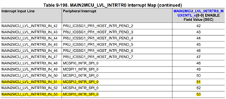
One question to consult, i want to use a GPIO interrupt in main domain in MCU, is it possible?
In mcusw it seems i can only access interrupt in MCU_R5FSS0 in MCU.
Looking forward to your kindly reply.
Thanks.
BR
Sihui Zhong
Hi Sihui,
What OS are you using on Linux A72, and what SDK version?
regards
Suman
Hello Suman,
We used QNX with pdk_jacinto_08_00_00_37.
BTW we tried to use MAIN2MCU_PLS_INTRTR0_OUTP to map the interrupt in main domain to mcu domain, however it doesn't work .
could you help to give some advice and guidance?
Thanks.
BR
Sihui
Hi,
Which GPIO instances are you using from main domain? You can only use MAIN_GPIO4 and MAIN_GPIO5 when running Linux on A72.
Regards,
Parth
Hello Parth,
we want to use GPIO0_43 to generate ISR in MCU domain.
pls let me know if any info needed to analyze the issue.
BTW we found MAIN2MCU_PLS_INTRTR0, not sure whether it could help to route main domain interrupt to related MCU domain.
here attached the code, but it didn't work.
/***************************************************USS1_DCR2B*************************************************************/
/* gpio module config: SOC2_USS1_DCR2B(GPIO_BANK2 | GPIO0_43) */
PortDrv_MainDomainPinMux(CSL_MAIN_CTRL_MMR_CFG0_PADCONFIG44, 0x08050007U, 0U);
/* gpio module config: SOC2_USS1_DCR2B(GPIO0_43) input */
regVal = CSL_REG32_RD(CSL_GPIO0_BASE + 0x38U); //GPIO_DIR23
regVal |= (1U << 0x0BU);
CSL_REG32_WR(CSL_GPIO0_BASE + 0x38U, regVal);
/* enables rising edge detection */
regVal = CSL_REG32_RD(CSL_GPIO0_BASE + 0x4CU); //GPIO_SET_FAL_TRIG23
regVal |= (uint32)(1U << 0x0BU);
CSL_REG32_WR(CSL_GPIO0_BASE + 0x4CU, regVal);
/* enables falling edge detection */
regVal = CSL_REG32_RD(CSL_GPIO0_BASE + 0x54U); //GPIO_SET_FAL_TRIG23
regVal |= (uint32)(1U << 0x0BU);
CSL_REG32_WR(CSL_GPIO0_BASE + 0x54U, regVal);
/* route MAIN2MCU_PLS_INTRTR0_OUTP_0 interrupt to MCU_R5FSS0_CORE0_INTR_IN_224 */
regVal = CSL_REG32_RD(MAIN2MCU_PLS_INTRTR0_MUXCNTL_0); //MAIN2MCU_PLS_INTRTR0_MUXCNTL_0
regVal = (regVal | (uint32)(0x3F)) & (uint32)(0x50U); //MAIN2MCU_PLS_INTRTR0_IN_79 --- GPIOMUX_INTRTR0_OUTP_16
/* enable input */
regVal |= (uint32)(0x10000U);
CSL_REG32_WR(MAIN2MCU_PLS_INTRTR0_MUXCNTL_0, regVal);
/* route GPIO0_43 interrupt to GPIOMUX_INTRTR0_OUTP_16 */
#if 1
regVal = CSL_REG32_RD(GPIOMUX_INTRTR0_INTR_ROUTER_MUXCNTL_16); //GPIOMUX_INTRTR0_MUXCNTL_16
regVal = (regVal | (uint32)(0xFF)) & (uint32)(0x2BU); //0-8 43
/* enable input */
regVal |= (uint32)(0x10000U);
CSL_REG32_WR(GPIOMUX_INTRTR0_INTR_ROUTER_MUXCNTL_16, regVal);
#endif
/* clear GPIO0_43 interrupt flag */
regVal = CSL_REG32_RD(CSL_GPIO0_BASE + 0x5CU);
CSL_REG32_WR(CSL_GPIO0_BASE + 0x5CU, regVal);
/* Per bank interrupt enable - bank2 */
regVal = CSL_REG32_RD(CSL_GPIO0_BASE + 0x8U);
regVal |= (uint32)(0x04U);
CSL_REG32_WR(CSL_GPIO0_BASE + 0x8U, regVal);
Thanks.
BR
Sihui
Hey,
As far as I know GOIO0 is owned by Linux/QNX by default. I am not sure if it can be used out of box. Looping in QNX experts for help.
Regards,
Parth
Hello Parth,
we can access this GPIO interrupt resource of main domain in MCU domain via register MAIN2MCU_PLS_INTRTR0, now it works.
but we still need to use SPI3 and SPI5 interrupt of main domain in MCU domain, any advice or experience?
thanks.
BR
Sihui
Hi Sihui,
Have you tried a similar approach for the SPI3 / SPI5 using MAIN2MCU_LVL_INTRTR0, as per below diagram from TDA4VM TRM Section 12.1.5.3.2 McSPI Integration in MAIN Domain?
Regards,
kb
Hello KB,
We have tried SPI3/SPI5 with using MAIN2MCU_LVL_INTRTR0. The interrupt ID is 211 for SPI3 and 213 for SPI5. But it didn't work.
Here attached the code,
#define MAIN2MCU_LVL_INTRTR0_MUXCNTL_51 (CSL_MAIN2MCU_LVL_INTRTR0_CFG_BASE + 0xD0)
#define MAIN2MCU_LVL_INTRTR0_MUXCNTL_53 (CSL_MAIN2MCU_LVL_INTRTR0_CFG_BASE + 0xD8)
/* route MCSPI3_INTR_SPI_0 interrupt to MCU_R5FSS0_CORE0_INTR_IN_211 */
regVal = CSL_REG32_RD(MAIN2MCU_LVL_INTRTR0_MUXCNTL_51); //MAIN2MCU_LVL_INTRTR0_MUXCNTL_51
regVal = (regVal | (uint32)(0x1FF)) & (uint32)(0x33U); //MAIN2MCU_LVL_INTRTR0_IN_51 --- MCU_R5FSS0_INTR_IN_211
/* enable output */
regVal |= (uint32)(0x10000U);
CSL_REG32_WR(MAIN2MCU_LVL_INTRTR0_MUXCNTL_51, regVal);
/* route MCSPI5_INTR_SPI_0 interrupt to MCU_R5FSS0_CORE0_INTR_IN_213 */
regVal = CSL_REG32_RD(MAIN2MCU_LVL_INTRTR0_MUXCNTL_53); //MAIN2MCU_LVL_INTRTR0_MUXCNTL_53
regVal = (regVal | (uint32)(0x1FF)) & (uint32)(0x35U); //MAIN2MCU_LVL_INTRTR0_IN_53 --- MCU_R5FSS0_INTR_IN_213
/* enable output */
regVal |= (uint32)(0x10000U);
CSL_REG32_WR(MAIN2MCU_LVL_INTRTR0_MUXCNTL_53, regVal);
pls let me know if any info needed to analyze the issue.
Thanks.
BR
Zachary
Hi KB,
Do you have any updates or ideas here, please let me know.
Thanks.
BR
Zachary