This thread has been locked.

If you have a related question, please click the "Ask a related question" button in the top right corner. The newly created question will be automatically linked to this question.

AM6442: How many PRU clock cycles does PRU assembly instruction SBBO, LBBO cost?

Part Number: AM6442


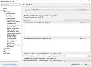
There's some explanation here 

https://e2e.ti.com/support/processors-group/processors/f/processors-forum/1051981/am6442-does-the-icssg1-pru0-supports-assembly-instruction-dmb-dsb-isb

But I found some different instruction representations.

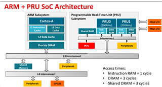
Sometimes LBBO takes 3 clock cycles to get the first 4 bytes of data from PRU internal memory, but sometimes it takes 4 clock cycles to do the same thing. That makes me supper confused.

I want to know what factors will affect the clock cycles took by LBBO?


  • Hello,

    What test are you running? Have you ensured that there is no arbitration delay on the bus from other PRU cores or system cores accessing the same memory?

    It looks like the thread you linked got lost in my inbox. Do I need to re-open it?

    Regards,

    Nick

  • Hi Nick,

    Here's parts of the test code. It's used to send a number of bytes to PRU GPIO at a fixed frequency.

    "LDI R30.b2, 0x1 \n\t "
    "LBBO &R29, R15, 0, 4 \n\t " /*LBBO load first 4 bytes will cost 3 system clk. But sometimes it seems cost 4 system clks*/
    "nop \n\t "
    "CLR R30, R30, clk_pin \n\t "
    "nop \n\t "
    "nop \n\t "
    "nop \n\t "
    "nop \n"
    "loop: \n\t "
    "MOV R30.b0, R29.b0 \n\t "
    "LDI R30.b2, 0x9 \n\t "
    "nop \n\t "
    "nop \n\t "
    "nop \n\t "
    "nop \n\t "
    "nop \n\t "
    "CLR R30, R30, clk_pin \n\t "
    "nop \n\t "
    "nop \n\t "
    "nop \n\t "
    "nop \n\t "
    "MOV R30.b0, R29.b1 \n\t "
    "SET R30, R30, clk_pin \n\t "
    "nop \n\t "
    "nop \n\t "
    "nop \n\t "
    "nop \n\t "
    "nop \n\t "
    "CLR R30, R30, clk_pin \n\t "
    "nop \n\t "
    "nop \n\t "
    "nop \n\t "
    "nop \n\t "
    "MOV R30.b0, R29.b2 \n\t "
    "SET R30, R30, clk_pin \n\t "
    "nop \n\t "
    "nop \n\t "
    "nop \n\t "
    "nop \n\t "
    "nop \n\t "
    "CLR R30, R30, clk_pin \n\t "
    "nop \n\t "
    "nop \n\t "
    "nop \n\t "
    "nop \n\t "
    "MOV R30.b0, R29.b3 \n\t "
    "SET R30, R30, clk_pin \n\t"
    "ADD cnt.w0, cnt.w0, 4 \n\t "
    "ADD cnt.b2, cnt.b2, 2 \n\t "
    "nop \n\t "
    "nop \n\t "
    "nop \n\t "
    "CLR R30, R30, clk_pin \n\t "
    "LBBO &R29, R15, cnt.w0, 4 \n\t "
    "QBGT loop, cnt.b2, output.b0 \n\t " /* if cnt.b2 < R28.b0(len), continue to read */
    "LDI R30.b2, 0x1 \n\t "
    "LDI R30.b0, 0 \n\t "
    "nop \n\t "
    "nop \n\t "
    "nop \n\t "
    "nop \n\t "

    From the code view, there's not any other PRU core or system core accessing the same memory. Is there any other methods to confirm this?

    We can discuss about it here, so you don't have to reopen the link thread, thank you! 

    Best Regards

    xixiguo

  • Hello xixiguo,

    Clock cycles to execute LBBO 

    I double-checked with the engineer who designed the PRU-ICSS. He said that all the information presented about LBBO at  https://e2e.ti.com/support/processors-group/processors/f/processors-forum/1051981/am6442-does-the-icssg1-pru0-supports-assembly-instruction-dmb-dsb-isb/3892729#3892729 was correct. His best guess was that arbitration delay was impacting your read time.

    Clock cycles to execute SBBO 

    The information I provided about SBBO in the above post was partially correct. SBBO writes to memory locations outside of the PRU subsystem will only take one PRU clock - the PRU spends one clock writing to the system bus buffer, and then moves on to the next assembly instruction. HOWEVER, the bus inside the PRU subsystem does not have any buffers. This means that an SBBO write to a location within the PRU subsystem takes one clock cycle, plus any arbitration delay if another core is using the bus. See my edited reply in the link above for more information.

    Next steps for testing 

    1) ensuring that other cores are not accessing PRU memory:
    If the other PRU_ICSSG cores are not running any firmware, then you know that they will not be accessing the PRU bus. If you are not instructing the A53 / R5F / M4F cores to access PRU memory space, I would expect that they would not cause arbitration delays. However, you could be super sure that the A53, R5, etc are not trying to access the PRU by just loading the PRU cores through CCS instead of a Linux or RTOS core. More information at https://e2e.ti.com/support/processors-group/processors/f/processors-forum/1045297/faq-am64x-am24x-how-to-use-code-composer-studio-ccs-to-connect-to-pru_icssg 

    2) ensuring that your test code is actually doing what you think it is doing:
    Assembly instructions are literally the PRU instructions that the PRU core runs. So there should be no "compilation" that reorders the assembly instructions around. With that said, the C compiler WILL potentially reorder your C code as a part of the optimization process.

    If you want to make sure the generated assembly code is actually doing what you think it is doing, you can actually keep the ASM file that is generated by the C compiler. just use C code compile option --keep_asm as in the image below:

    Regards,

    Nick

  • Another option is to just write your assembly instruction test code in an assembly project without any C code. You can use the getting started labs in the PRU Software Support Package (PSSP) as a template.

  • Hi Nick,

    Thank you for double confirm my question with the hardware engineer!

    It seems the main factor that effect the LBBO and SBBO is the ICSS bus.

    From this architecture picture, it seems that PRU access memory locations outside of the PRU subsystem still needs to across the interconnect bus. If so, it also will be influenced by the bus arbitration delay, right?

    Is there any method can order the bus access priority? Such as specifies that PRU0 has the highest priority?

    Best Regards

    xixiguo

  • I use CCS project to ensure that only ICSSG1 PRU0 runs. And I also modified the project properties with C code compile option --keep_asm be checked.

    But I get the result that LBBO sometimes costs 4 PRU clk when load 4 bytes from PRU0 data memory. This occurs when the LBBO load from a non 4 bytes aligned address in PRU0 data memory. If the address is 4 bytes aligned, LBBO takes 3 PRU clk.

    I also test SBBO, but I found that SBBO store 4 bytes data takes 2 PRU clk to action when destination address is 4 bytes aligned. It will cost 1 more PRU clk when the destination address is not 4 bytes aligned.

  • Hello xixiguo,

    Good questions!

    Interconnects

    The AM64x Technical Reference Manual (TRM) is not clear on whether PRU/RTU/TX_PRU cores use the internal CBASS interconnect to access the system CBASS0 interconnect, or whether there are two different connection points. My assumption is that there are two separate connection points, since AM64x PRU_ICSSG is very similar to AM65x PRU_ICSSG (for key differences, future readers reference https://www.ti.com/lit/sprac90 ). From the AM65x PRU_ICSSG TRM chapter, we see that the external system CBASS0 connection is separate from the 32-bit internal CBASS interconnect:

    Let me double-check with the designer. I have filed a ticket with the documentation team to add a similar graphic to the AM64x TRM (timeline to fix TBD).

    4 byte alignment impact on internal CBASS accesses? 

    Good testing! Let me check with the designer on whether this is expected.

    Regards,

    Nick

  • Hello xixiguo,

    Ok, this is going to be a long one. We are going to go SUPER in depth here. I am also going to rewrite my response from your previous thread to try to integrate the new information. This is accurate to my current understanding, but if I need to edit information going forward I'll mark it in RED.

    Read / Write Latencies for PRU-ICSS devices

    the PRU Assembly Instruction User Guide (https://www.ti.com/lit/spruij2) describes every PRU assembly instruction. For our discussion on read & write latencies, we will focus on LBBO (reads) and SBBO (writes). Whenever I say "word" below, I am talking about 32 bit words.

    This information supplements the PRU Read Latencies App note (https://www.ti.com/lit/sprace8 ). Future readers, this information may have already been added to the app note by the time you are reading this post.

    These basic rules apply:

    1) all PRU instructions that are not memory reads or writes execute in a single PRU clock cycle

    2) PRU writes to memory locations outside of the PRU subsystem take N PRU clocks for SBBO to write N words
     * these instructions are fire-and-forget.
     * There are buffers between the PRU subsystem and the rest of the device. It takes N clock cycles for SBBO to write N words to the system bus buffer. Then the PRU will move to the next assembly command without waiting for the write to complete. It will take additional time for the value written to the buffer to travel through the system busses and eventually update the external memory address.
     * This assumes that the SBBO writes are to addresses that are word aligned (e.g., 0x100, 0x104, 0x108, etc). Whenever the load crosses a 4 byte boundary, it takes another PRU clock cycle.
       - e.g., write 2 bytes to 0x100: one PRU clock
       - e.g., write 2 bytes to 0x102: one PRU clock
       - e.g., write 2 bytes to 0x103: two PRU clocks (one clock to write to the word at 0x100, one clock to write to the word at 0x104)
     * Thus, if the write address is not word aligned, the equation changes to N + 1 PRU clocks for SBBO to write N 32-bit words

    3) PRU write instructions to memory locations within the PRU subsystem take N PRU clocks for SBBO to write N words, plus arbitration delay
     * This is because there are no buffers between the PRU core and memory internal to the PRU subsystem. Thus, if another core is using a peripheral or memory connected to the ICSS CBASS bus, the PRU core has to wait for the peripheral or memory to become available before it can perform a write.
     * Note that internal CBASS interconnect is "fully switched". That means that multiple cores can use the CBASS simultaneously, as long as they are accessing different peripherals or memories. e.g., PRU0 can access DRAM at the same time that PRU1 is accessing the PRU's hardware UART.
     * See the "deep dive on arbitration delay" section below for information on how to calculate arbitration delay.
     * The same word alignment rules from 2) apply here. i.e., if the write is not word aligned, add 1 additional clock cycle.

    4) PRU read instructions will take multiple PRU clock cycles, depending on how far away the destination memory is. Reads from memory locations within the PRU subsystem may have arbitration delay.
     * 
    See the "deep dive on LBBO & DRAM" section below
     * The same word alignment rules from 2) apply here. i.e., if the read is not word aligned, add 1 additional clock cycle.

    Read / Write Latencies for PRU_ICSSG devices 

    1) is the same

    2) Write latency to memory locations outside the PRU subsystem are same as for PRU-ICSS, but add per-slice arbitration delay
     * See the arbitration delay sections below

    3) Write latency to memory locations inside the PRU subsystem are the same as for PRU-ICSS 
     * Note that there is still one single internal CBASS per ICSSG. So cores that are in different slices will still deal with arbitration delay if they are trying to access the same peripheral or memory at the same time

    4) Read latency follows similar rules as PRU-ICSS, but add per-slice arbitration delay
    * See the arbitration delay sections below

    Deep dive on LBBO & DRAM 

    LBBO from PRU DRAM takes 2 + N PRU clocks to read N words (plus arbitration delay, plus 1 PRU clock if address is not word aligned)

    LBBO takes 3 clock cycles to get the first 4 bytes of data from PRU internal memory. Every additional 4 bytes adds 1 clock.
    for example,  LBBO loadDestination, loadAddress, 0, 16
    takes 6 PRU clocks: 3 clocks to load the first 4 Bytes, and 3 clocks to load the next 12 Bytes

    Arbitration delay

    Arbitration on the internal CBASS

    Any time a PRU core performs a load or store (i.e., read or write) from an endpoint in the internal CBASS, there is a chance that another core is already accessing that endpoint. An endpoint can be a peripheral, or a memory. Separate memories act as separate endpoints (e.g., one core can access DMEM0, one core can access DMEM1, and another core could access SRAM simultaneously).

    The internal CBASS bus is 4 Bytes wide. This applies to all PRU-ICSS and PRU_ICSSG devices. So if another core is performing an atomic write of x Bytes then it will take ceil(x/4) PRU clocks for the write to occur. E.g., a write of 30 bytes would take ceil(30/4) = ceil(7.5) = 8 PRU clocks to complete.

    If a PRU core and a non-PRU core (e.g., Linux A53 or RTOS R5) try to access the same ICSS/ICSSG location during the same PRU clock cycle (SRAM, UART, ECAP, etc), the PRU wins. However, if PRU initiates a transaction from SRAM after another core is executing a burst write transaction, the PRU transaction will stall until the burst write is completed. So if the non-PRU core's write takes 8 PRU clocks to complete, the longest the PRU would have to wait is 8 - 1 = 7 PRU clocks. If you want to completely avoid arbitration delay, you could program the non-PRU core to perform multiple 4 Byte writes instead of a single long write. In that case, the PRU would win arbitration every clock cycle it initiates a read.

    If two PRU cores try to access the same ICSS/ICSSG location during the same PRU clock cycle, then PRU0 wins (except for DMEM1, where PRU1 wins). I am still waiting for additional details about arbitration on the internal CBASS for PRU_ICSSG cores.

    Note that accesses to the external CBASS are totally separate from accesses to the internal CBASS. That means that reads or writes over the internal CBASS are unaffected by reads or writes over the external CBASS.

    Arbitration to the external CBASS (PRU_ICSSG only)

    PRU-ICSS cores will not experience arbitration delay when trying to access the external system CBASS. However, PRU_ICSSG is slightly different. Within an ICSSG slice, the PRU, RTU, and TX_PRU have a choke point before the signals reach the external CBASS. Thus, if one of the other cores in the slice is using the external CBASS for a read or a write, the core needs to wait until the bus becomes available. The interface to the external CBASS is 4 Bytes wide, so the math to calculate arbitration delays to the external CBASS is the same as calculating arbitration delays to the internal CBASS. The See the internal CBASS discussion of arbitration delay for how to calculate the arbitration delay for an atomic read or write.

    If multiple PRU_ICSSG cores try to access the external CBASS at exactly the same clock cycle, arbitration priority is: PRU first, then RTU, then TX_PRU.

    There is NOT a choke point across slices. e.g., if ICSSG1_PRU0 is using the external CBASS, then ICSSG1_PRU1 is NOT affected by arbitration delay since it is in a separate slice.

    CBASS Bus structure 

    AM64x & AM65x have the same bus structure. Please reference the figure discussed in my previous response.

    Regards,

    Nick

  • Hello,

    The above post has been edited. Changed text in RED. The above post will be turned into an FAQ here:

    https://e2e.ti.com/support/processors-group/processors/f/processors-forum/1096933/faq-pru-how-do-i-calculate-read-and-write-latencies

    Regards,

    Nick

  • Hi Nick,

    Thanks for reply.

    That means that multiple cores can use the CBASS simultaneously, as long as they are accessing different peripherals or memories.

    Does this mean PRU0 can access Data Memory0 while at the same time PRU1 can access Data Memory1. And PRU0&PRU1 both does not have any arbitration delay?

    If so, how does the CBASS manage this? Does this mean that the CBASS is not a a simple 32bits bus, it also has a control unit to achieve this feature?

    Is there any document to introduce the CBASS working mechanism?

    Best Regards

    xixiguo

  • Hello Xixiguo,

    That is correct. As long as PRU0 and PRU1 are accessing different endpoints (and DMEM0, DMEM1, SMEM are all different endpoints), there is no arbitration delay. Let me know if you would reword anything in https://e2e.ti.com/support/processors-group/processors/f/processors-forum/1096933/faq-pru-how-do-i-calculate-read-and-write-latencies/4065864#4065864 section "Arbitration delay" to make that easier to understand.

    The CBASS bus inside of the PRU subsystem is "fully switched".

    What does that mean? Let's compare the CBASS to a mux: each core (or the access point for a core external to the PRU subsystem) could be thought of as an input, and each endpoint (memory, peripheral, etc) can be thought of as an output. As long as input1 and input2 are being muxed to different outputs, there is absolutely no interference.

    Regards,

    Nick