


Other Parts Discussed in Thread: SN74AVC4T774
We have followed the instructions to compile, load and use the IBL for the C6657 EVM and have been able to load an application onto the board and boot the application.
[https://e2e.ti.com/support/processors-group/processors/f/processors-forum/1057566/faq-tms320c6657-how-to-flash-the-ibl-intermediate-boot-loader-into-eeprom-and-how-to-flash-the-application-binary-into-nor-how-to-boot-the-ibl-application-binary]
We are now progressing to our own custom hardware. Our initial hardware has a similar memory map to the EVM (i.e. I2C EEPROM, SPI FLASH, DDR3). The main difference is that our DDR3 memory requires a different setting for the DDR3 configuration for proper operation.
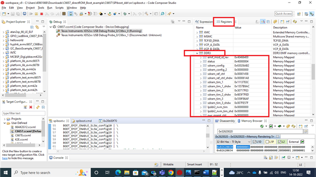
Our first step was to modify the EVMs GEL file to properly configure our hardware. With these changes we have properly configured the DDR3 memory and have verified the processor is running and able to debug an application.
The next step is to modify the IBL/RBL configurations to use these changes. We are attempting to emulate the EVMs boot characteristics. (i.e. load the IBL from I2C EERPOM and the application from SPI FLASH.) However, we are struggling to determine where/how to accomplish this task.
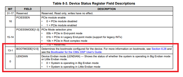
- Are there any documentation/application notes/instructions/examples that show where/how to modify/configure the IBL to properly configure the DDR3 interface before loading the application?
- Is it possible to load from SPI Flash directly with the RBL? (i.e. boot the processor directly from the SPI FLASH.) If possible, are there any documentation/application notes/instructions/examples that show where/how to modify/configure the RBL to properly configure the DDR3 interface before loading the application?


 (Stopped on some random address.)
 (ie. the expected results)


 The PC appears to be stuck in the RBL.


