


Part Number: TMS320C6657
Hi team,
Here're 2 questions from the customer may need your help:
1) Debug the PCIE interface using the PCIE example as follows:
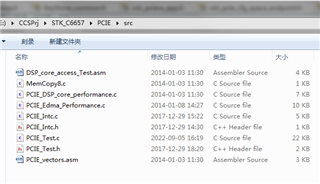
PCIE EP side reading and writing issue is as follows:
In RC mode, connect an EP device; at initialization, you can see that EP has a 64-bit bar space, 16 KB in length, using bar0 and bar1. The software then assigns the PCIe space address to bar0 and bar1.
The allocated address space starts with #define PCIe_NONFETCH_base_address 0x10000000 and corresponds to an outbound region0. All three registers are configured as per the routine and are unchanged.
After the configuration is complete, in the final PCIe_Test function, the bar0 bar1 on the EP side is read and printed from the remote register and the three register values for region 0 are read and printed:
ulData = *(volatile uint32_t *)(CSL_PCIE_CONFIG_REGS + 0x2010); // bar0
uart_printf ("EP configuration register bar0 = %x\n\n",ulData);
ulData = *(volatile uint32_t *)(CSL_PCIE_CONFIG_REGS + 0x2014); // bar1
uart_printf ("EP configuration register bar1 = %x\n\n",ulData);
//outbound region related register
ulData = gpPCIE_app_regs->OB_SIZE;
uart_printf ("rc app register OB_SIZE = %x\n\n",ulData);
ulData = gpPCIE_app_regs->OUTBOUND_TRANSLATION[0].OB_OFFSET_HI;
uart_printf ("rc app register OB_OFFSET_HI 0 = %x\n\n",ulData);
ulData = gpPCIE_app_regs->OUTBOUND_TRANSLATION[0].OB_OFFSET_INDEX;
uart_printf ("rc app register OB_OFFSET_INDEX 0 = %x\n\n",ulData);
Printed results are as follows:
EP configuration register bar0 = 10000004
EP configuration register bar1 = 0
rc app register OB_SIZE = 3
rc app register OB_OFFSET_HI 0 = 0
rc app register OB_OFFSET_INDEX 0 = 10000001
At this point, the software tests if it can read the bar space of EP by accessing 0x60000000 again:
// Test bar mem space read and write
unsigned int value = *((volatile Uint32 *)0x60000008);
When this sentence is executed, the software triggers an exception(they are suspecting NMI/exception in PCIe_vector.ASM)
interrupt vector table
.sect "vecs"
.align 1024
vectors:
VEC_RESET _c_int00 ;RESET
VEC_ENTRY NMI_ISR ;NMI/Exception
VEC_DUMMY ;RSVD
VEC_DUMMY ;RSVD
VEC_ENTRY PCIE_MSI_ISR ;interrupt 4
VEC_ENTRY PCIE_ERR_PMRST_ISR ;interrupt 5
This bar space in the peer EP device is the configuration register of the nvme device itself and is readable.
2) Regarding the section 3.2.3 PCIe Inbound Address Translation Examples in PCIe Use Cases for KeyStone Devices,

The EP side initiates an inbound read and write to RC, is the EDMA on the RC side not involved? If without DMA, is read-write efficiency low? Or implemented by the DMA of the EP end device?
Also, could you help check if the understanding of outbound and inbound is correct:
Outbound : C6657 initiates read and write to EP as RC and uses outbound for address translation.
Inbound: C6657 as RC, EP initiates read and write to RC and uses inbound for address translation.
Could you help check this case? Thanks.
Best Regards,
Cherry

