This thread has been locked.

If you have a related question, please click the "Ask a related question" button in the top right corner. The newly created question will be automatically linked to this question.

J721EXSOMXEVM: PCIe Root Complex Initialization Steps

Part Number: J721EXSOMXEVM
Other Parts Discussed in Thread: DRA829, TDA4VM, TCA9543A, CDCI6214, TCA6416A, TCA6424, TCA6416

Hi 

Is there any developer guide exist for PCIe Root complex initialization sequence on TDA4VMXEVM (J721E DRA829/TDA4VM Processors).

Particularly, How SerDes0 configuration or initialization for PCIe is performed. 

Regards 

  • HUQ, 

    There is no such documentation unfortunately. You best reference is the Linux device driver source code. From the high-level, below are the steps:

    1. Setup_serdes for PCIe 
    2. Enable lanes, check for PLL lock.  
    3. Setup PCIe controller
    4. Start PCIe link, poll for link status
    5. Once linked, enumerate device

    Hope this can give you some guidance to navigate the linux driver source code, which are located under:

    Cadence SERDES driver: 

        <LinuxSDK>board-support/linux-5.10.120+gitAUTOINC+95b90aa828-g95b90aa828/drivers/phy/cadence/phy-cadence-sierra.c

    TI WIZ wrapper for SERDES: 

       <LinuxSDK>board-support/linux-5.10.120+gitAUTOINC+95b90aa828-g95b90aa828/drivers/phy/ti/phy-j721e-wiz.c

    Cadence controller driver:

       <LinuxSDK>board-support/linux-5.10.120+gitAUTOINC+95b90aa828-g95b90aa828/drivers/pci/controller/cadence

    please let us know if there are further information that we can help. 

    regards

    jian

  • Thanks Jian for your feedback. Appreciated. 

    Regarding SerDes0 for PCIe0, I think, we need to unlcok/lock Partition 1 (not the Partition 0) before SerDes initialization. 

    As per TRM Section  5.1.3.4.137: LOCK1_KICK0 unlock value is 0x68EF3490

    As per TRM Section  5.1.3.4.138: LOCK1_KICK1 unlock value is 0xD172BC5A

    For more information, see TRM Section  5.1.3.3.1.2 Kick Protection Registers

    Can you confirm above unlock values. Moreover, what will be the lock values? 

    Regards 

  • HUQ, 

    the KICK register pairs are for CTLMMR registers only. i.e., CTRLMMR_SERDES0_LN0_CTRL, CTRLMMR_SERDES0_LN1_CTRL, they are located at 0x00104080 and 0x00804084. These requires KICK unlock sequence. For SERDES0 IP level registers, with offset 0x05000000, you do not need KICK registers. 

    To lock MMR regions, you simply write a non-key value to the KICK0 register, then verify the log bit. And I can confirm the Partition 1 locks is the right ones for the SOC level MMRs that controls SERDES lane mux. Additionally, CTRLMMR_SERDES0_CLKSEL and CTRLMMR_SERDES0_CLK1SEL are at address 0x00108400 block, which you will need to operate LOCK2 region KICKs. 

    Jian

  • Hi Jian, 

    Thanks for your information regarding LOCK registers. 

    Initialized CTRL MMR, SERDES and PCIE modules but still PCIE0 (PCIe x1 lane - J11) Root Complex (TDA4VMXEVM) is not Link UP. PCIE_USER_LINKSTATUS still informs "No receivers detected". As per your guidelines, performed following steps. 

    1. Selected PCIE0 via I2C Mux (TCA9543A)
    2. Low the 6th Pin "PCIe_1L_RC_RSTz" for 2ms and the high it again via I2C Expander-1 (TCA6416ARTWR)
    3. CTRLMMR_PCIE0_CTRL = 0x82
    4. Clock Initialization (TI SCI Firmware & Platform Level)
    set_device (239, 2, 0)
    enable_clk_state (239, 1) // DEV_PCIE0 = 239
    set_device(292, 2, 0);//DEV_SERDES_16G0 = 292
    set_clk_parent(292, 11, 15);
    enable_clk_state(292, 11);
    set_clk_parent(292, 0, 4);
    enable_clk_state(292, 0);


    Based on your comment on a thread: e2e.ti.com/.../dra829v-dra829-enabling-of-pcie-ref-clk-in-qnx

    CTRLMMR_PCIE_REFCLK0_CLKSEL = 0x100
    CTRLMMR_ACSPCIE0_CTRL = 0x01000000
    CTRLMMR_ACSPCIE1_CTRL = 0x01000000
    SERDES_TOP_CTRL = 0x9A000000
    SERDES_RST = 0xB1000000
    SERDES_LANECTL0 = 0x73000000
    CTRLMMR_SERDES0_CLKSEL = 3
    CTRLMMR_SERDES0_LN0_CTRL = 1
    CTRLMMR_SERDES0_LN1_CTRL = 1
    PCIE_USER_CMD_STATUS = 1

    but no success. Still unable to link up the PCIe Root Port. 

    Can you confirm above steps? 

    Promptly response will help a lot. 

  • Hi Jian, 

    Have you get a time to see above question. 

  • HUQ, 

    Sorry for the delayed response. I see you are using the PCIe0 slot on the EVM. Can you confirm if you the REFCLK on the PCIe slot was already toggling, on your Step 2:

    >>2. Low the 6th Pin "PCIe_1L_RC_RSTz" for 2ms and the high it again via I2C Expander-1 (TCA6416ARTWR) 

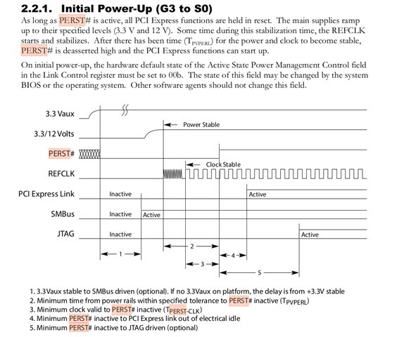
    PCIe spec requires the clock being stable before you deasserting the PERST (pulling reset high). I attached the diagram from the PCIe CEM spec below, but you can look up detailed timing requirement in the original spec.

    /resized-image/__size/320x240/__key/communityserver-discussions-components-files/791/pastedimage1671039721286v1.png

    Additionally, can you confirm what kind of card you plugged into the slot? please note this is public forum. 

    Jian

  • Hi Jian, 

    How can we check the toggling of refclk. Is there any test point on board? 

    Increased the delay to 100ms between low and high of pin but no success. No action is performed during the delay. 

    Card: USB controller: Fresco Logic FL1000G USB 3.0 Host Controller (rev 01)

    HUQ

  • HUQ, 

    The default resistor configuration on the EVM uses a clock generator device to supply the refclk to both the RC and EP. So unless you modified the EVM, you should NOT enable ACSPCIe pads. Otherwise, they may drive signals that interfere with the clkgen output. So you should leave below registers to default:

       CTRLMMR_ACSPCIE0_CTRL = 0x01000003
       CTRLMMR_ACSPCIE1_CTRL = 0x01000003

    So let's verify the clocking configuration:

    1. The USB controller card requires refclk, that is sourced from the clkgen device CDCI6214, which:

           - is reset by the signal "SOC_PORZ_OUT" - no software control needed.

           - CDCI1_OE3/4 enabled clk signals, they should be driven by the I2C GPIO Expander1. 

          you may need to check the Linux code on if/how the CDCI6214 is programmed to output 100Mhz refclk. I have look into that portion of the driver for the EVM. 

    2. On the RC (TDA4) side, though the refclk is provided to the SERDES from external, the default SDK linux driver uses internal refclk generated by the on-chip PLL.  I see you have (assumed these are read-back values):

        CTRLMMR_PCIE_REFCLK0_CLKSEL = 0x100 (incorrect)  //this should be set back to 0x0, disable output refclk. but not critical as you already disabled pins. 

        CTRLMMR_SERDES0_CLKSEL = 3 (correct) //using MAIN_PLL2_HSDIV4_CLKOUT

        SERDES_RST = 0xB1000000 (correct) //using cmn_refclk_int and cmn/refclk1_int


        please also check register PHY_PMA_CMN_CTRL, to see if one of the PLLs locked. 

    In your system, the RC did not detect any receiver. This is likely cause by the fact that the USB controller card is either not powered up, not clocked, or, still in reset and did not enter LTSSM state. 

    To physically measure the refclk supplied the card, you may probe A13/A14 pins on J11, or R109/R110 0Ohm resistors that connected to the PCIe slot.Note that you will need to scope that is capable to 100MHz signal.  

    I also attached a snapshot of the schematics. 

    Jian

  • Hi Jian,

    Thanks for your valuable feedback.

    Please note that we are using TDA4VMXEVM board without any hardware modification. On same board, used Linux image and I can see the result of lspci command. We are not using Linux or QNX or any other SDK. Only uboot is used.

    We are using default external clock generator that supply refclk to the PCIe slot and TDA4VM SOC. I have also scanned the thread
    e2e.ti.com/.../faq-tda4vm-tda4vm-dra829v-routing-pcie-reference-clock-externally
    and it is assumed that there is no need to implement the patch mentioned in this thread.

    1. Since no hardware medication is performed so used these settings
    SERDES_RST = 0
    SERDES_TOP_CTRL = 0x9A000000
    SERDES_RST = 0x31000000
    SERDES_LANECTL0 = 0x73000000
    SERDES_LANECTL1 = 0x33000000
    SERDES_RST = 0xB1000000

    CTRLMMR_ACSPCIE0_CTRL = 0x01000003
    CTRLMMR_ACSPCIE1_CTRL = 0x01000003
    CTRLMMR_PCIE_REFCLK0_CLKSEL = 0
    CTRLMMR_PCIE_REFCLK1_CLKSEL = 1
    CTRLMMR_SERDES0_CLKSEL = 3
    CTRLMMR_SERDES0_CLK1SEL = 3
    CTRLMMR_SERDES0_LN0_CTRL = 1
    CTRLMMR_SERDES0_LN1_CTRL = 1
    CTRLMMR_PCIE0_CLKSEL = 0

    2. Already did following configurations on I2C MUX and I2C GPIO Expanders.
    TCA9543A: Set value 1 (Enabled PCIe 0 only)
    TCA6416A: Clear, Delay (100ms) and then set PCIE_1L_RC_RSTZ (Output Port 0, Bit 6)
    TCA6424 : Clear, Delay (2ms) then set PCIe_CLKREQn_MUX_SEL (Output Port 1, Bit 6)
    TCA6416A: Clear, Delay (2ms) then set CDCI1_OE2/OE3 (Output Port 1, Bit 3)

    For PCIe_CLKREQn_MUX_SEL to be set in Expander, Also Set CTRLMMR_PADCONFIG134 (0x11c218) = 0x50007

    3.
    Regarding CDCI6214, As per User Guide:
    "In addition to the Primary clock, the SERDES reference clocks to the SoC is sourced from the Clock Generator (CDCI6214) on the Common processor board. All these clocks are 100 MHz with HCSL level for the SoC’s SERDES reference clock input. The programming of CDCI6214 chip is done through J721E SoC’s I2C0 port. There are two CDCI6214 clock generators available to source the SERDES reference clocks to SoC. The CDCI1 (U22) is not connected to I2C0 port by default. The clocks from CDCI1 (U22) is derived using factory programmed configuration."

    Should we need to configure CDCI6214? If yes, can you provide Linux reference for CDCI6214 that you have explored?

    4. Value of PHY_PMA_CMN_CTRL is 0x00002030

    Will post the result after scope of A13/A14 pins on J11.

    Regards

  • Just realized that you had mentioned both bits CDCI1_OE2/OE3 and  CDCI1_OE1/OE4. I have configured both in I2C GPIO expander but no success. PCIE_USER_LINKSTATUS is still zero. 

  • HUQ, 

    Your PHY_PMA_CMN_CTRL is 0x00002030, indicating none of the SERDES PLLs are locked. Can you confirm which function you called to setup SERDES for PCIe? you should be calling the Cadence API and WIZ API, similar to how they were called in Linux. 

    Jian

  • Also HUQ, 

    on you last comment: 

      >We are not using Linux or QNX or any other SDK. Only uboot is used.

    Can you clarify in your system:

    1. Which core/OS is designated to bring up the PCIe interface and enumerate the PCIe address space?
    2. Which core/OS will be using PCIe interface for data transfers?

    Since there are quite some driver software needed to bring up SERDES and PCIe, you will need to replicate what the Linux driver did for SERDES setup and PCIe enumeration. 

    Jian 

  • Thanks for your response 

    We are working on A72 Core and using proprietary RTOS. Uboot is used as a boot loader.  

  • What do you mean by Cadence and Wiz API?

    Regarding the clock and parent clocks of Wiz/Serdes/PCIe, following sequence is used 

    enable_clk_state(DEV_SERDES_16G0, DEV_SERDES_16G0_CLK);// 292, 5

    disable_clk_state(DEV_SERDES_16G0, DEV_SERDES_16G0_CORE_REF_CLK); 
    set_clk_parent(DEV_SERDES_16G0, DEV_SERDES_16G0_CORE_REF_CLK, DEV_SERDES_16G0_CORE_REF_CLK_PARENT_HSDIV4_16FFT_MAIN_2_HSDIVOUT4_CLK);// Module ID, Clock ID, Parent ID
    set_clk_freq(DEV_SERDES_16G0, DEV_SERDES_16G0_CORE_REF_CLK, 25000000);
    enable_clk_state(DEV_SERDES_16G0, DEV_SERDES_16G0_CORE_REF_CLK);

    disable_clk_state(DEV_SERDES_16G0, DEV_SERDES_16G0_CORE_REF1_CLK);
    set_clk_parent(DEV_SERDES_16G0, DEV_SERDES_16G0_CORE_REF1_CLK, DEV_SERDES_16G0_CORE_REF1_CLK_PARENT_HSDIV4_16FFT_MAIN_2_HSDIVOUT4_CLK);// Module ID, Clock ID, Parent ID
    set_clk_freq(DEV_SERDES_16G0, DEV_SERDES_16G0_CORE_REF1_CLK, 25000000);
    enable_clk_state(DEV_SERDES_16G0, DEV_SERDES_16G0_CORE_REF1_CLK);

    set_device (239, 2, 0x400)
    enable_clk_state (239, 1) // DEV_PCIE0 = 239

  • HUQ, 

    >>What do you mean by Cadence and Wiz API?

    There is a set of registers to be configured to prepare SERDES in PCIe mode and with the right speed etc. These registers are grouped as Cadence portion and WIZ portion (TI wrapper). Simply enable the clocks and setting muxes are not sufficient. I sent you pointers to these files in the previous post:

    Cadence SERDES driver: 

        <LinuxSDK>board-support/linux-5.10.120+gitAUTOINC+95b90aa828-g95b90aa828/drivers/phy/cadence/phy-cadence-sierra.c

    TI WIZ wrapper for SERDES: 

       <LinuxSDK>board-support/linux-5.10.120+gitAUTOINC+95b90aa828-g95b90aa828/drivers/phy/ti/phy-j721e-wiz.c

    Cadence controller driver:

       <LinuxSDK>board-support/linux-5.10.120+gitAUTOINC+95b90aa828-g95b90aa828/drivers/pci/controller/cadence

    but seems you have not viewed them yet. one approach may be to follow the Linux driver on how the SERDES APIs are called, and do the same steps. Need to warn you that this will be non-trivial effort as there are other functions related to linux device tree and probing.  

    regards

    Jian

  • Hi Jian, 

    I had already scanned these modules (Wiz, Serdes, Cadence) like some of the init are 

    https://elixir.bootlin.com/linux/latest/source/drivers/phy/cadence/phy-cadence-sierra.c#L2170

    https://elixir.bootlin.com/linux/latest/source/drivers/phy/cadence/phy-cadence-sierra.c#L2179

    It seems, some minor initialization is missing. Revisiting my code to find the missing bits. 

    Regards 

  • HUQ, 

    Your first sign of success should be bit 10 or 11 be set, indicating one of the internal PLL is locked, in register PHY_PMA_CMN_CTRL. 

    Let us know if you met further issues. 

    Jian

  • Hi Jian, 

    Tried to find platform initialization sequence of PCA9543, TCA6416, TCA6424 and CDCI6214RGET but no success. Can you guide?

  • Hi Jian, 

    Have you get a chance to see above question? 

  • Hi H@fiz,

    Unlocking the thread. Is this still an open issue? If yes, could you explain the significance of PCA9543, TCA6416, TCA6424 and CDCI6214RGET? I did not follow how these devices entered the discussion.

    My assumption for CDCI6214RGET is that since it is a clock generator, you were looking for how REFCLK should be initialized. In which case, I would recommend reading PCI Express Card Electromechanical Specification Revision 3.0.pdf section 2.2.1. Initial Power-Up. This is a standard document that could be obtained online for PCIe. For convenience, I will post the section here:

    According to this, and it's previous section 2.2, PERST# signal should be deasserted at least after 100ms (Tpvperl) and REFCLK should stabilize within this period. There was a recent patch to increase delays to match this specification that I would recommend trying out if the issue is still being seen for RC initialization: https://lore.kernel.org/lkml/20230707095119.447952-1-a-verma1@ti.com/

    Regards,

    Takuma