This thread has been locked.

If you have a related question, please click the "Ask a related question" button in the top right corner. The newly created question will be automatically linked to this question.

SK-AM64: Follow up question: How to read/write data with the PRU_ICSSG XFR2VBUS Hardware Accelerator

Part Number: SK-AM64

Hello,

i saw this forum post:

https://e2e.ti.com/support/processors-group/processors/f/processors-forum/954953/tmdx654idkevm-how-to-read-write-data-with-the-pru_icssg-xfr2vbus-hardware-accelerator/3570126?tisearch=e2e-sitesearch&keymatch=XFR2VBUS#3570126

that pointed to another forum post. 

https://e2e.ti.com/support/processors-group/processors/f/processors-forum/959089/tmdx654idkevm-how-to-use-xfr2vbus-commands-with-48-bit-addresses/3700145?tisearch=e2e-sitesearch&keymatch=XFR2VBUS#3700145

It seems like the original poster didn´t need the answer - but for me, especially question 5 is still relevant:

Quote:

"Question 5:

In several examples, I have seen the following macros for the Write implementation


m_xfr2vbus_write32 .macro xid, addr_low, addr_high

   ldi32 r10, addr_low

   ldi r11.w0, addr_high

   xout xid, &r2, 40

   .endm


m_xfr2vbus_write64 .macro xid, addr_low, addr_high

   ldi32 r18, addr_low

   ldi r19.w0, addr_high

   xout xid, &r2, 72

   .endm


These macros work perfectly. But if I change the following lines in macros:


m_xfr2vbus_write32: xout xid, &r2, 40 -> xout xid, &r2, 32

m_xfr2vbus_write64: xout xid, &r2, 72 -> xout xid, &r2, 64


they do not work.


Why do I have to specify a length of 40 for 32 bytes to be written and a length of 70 for 64 bytes to be written?

How will the xout command look like to write 1/4/8 bytes of data (What should be the argument length for xout command to write 1/4/8 bytes)? "

If there is allready further documentation on how to use the XFR2VBUS Hardware Accelerator correctly, i would be happy about a hint. Another question on this topic is:

Is it necessary to use assembly language to use the accelerator effectively?

(Until now i was abled to achieve good results with C-code in PRU projects under CCS 11.1.0 with the PRU C-Compiler v2.3.3)

regards,

Dominik

  • Hello Dominik,

    Thank you for the query.

    I am assigning to the expert. Please expect some delay.

    Regards,

    Sreenivasa

  • Hello Dominik,

    At this point, I have not done many experiments with xout beyond the basic "Direct Connect" example in the PRU Software Support Package (PSSP) which is written in C: https://git.ti.com/cgit/pru-software-support-package/pru-software-support-package/tree/examples/am64x/PRU_Direct_Connect0/PRU0_Direct_Connect.c . More documentation is in the C compiler user's guide, section "PRU Instruction Intrinsics"(https://www.ti.com/lit/spruhv7 ).

    No, it is not necessary to use assembly to use the XFR2VBUS. However, assembly can be useful for parts of your PRU code where you must know exactly what instruction the PRU is running at every single clock cycle (e.g., the bitbanging code where a PRU is reading & writing a custom protocol to the PRU GPO / GPI pins is often in assembly). If you need examples of mixing C code and assembly code, check out the PRU Getting Started Labs at https://software-dl.ti.com/processor-sdk-linux/esd/AM64X/08_04_01_04/exports/docs/common/PRU-ICSS/PRU-Getting-Started-Labs.html

    Are you observing similar behavior with the assembly? We do not currently document the need for an additional 8 bytes of padding in the PRU Assembly Instruction User Guide (https://www.ti.com/lit/spruij2 ). If the assembly documentation needs to be updated, please let us know and I'll file a ticket to make sure that gets done at some point.

    Regards,

    Nick

  • Hello Nick,

    thank you for your reply! I wasn't abled to verify the problem with the padding in assembly yet. But I managed to get the XFR2VBUS working with C-Code. Here is my test program used in the PRU RTU0 / 0:

    #define WR_ID0 0x62
    #define RD_ID0 0x60
    
    #define WR_BUSY 20
    #define WR_DATA 2
    #define WR_ADDR 10
    
    #define NO_REMAPPING 0
    
    #define DDR_START_ADDRESS ((uint32_t)0x80000000)
    
    int main(void)
    {
        uint64_t testdata = 0x5555AAAA5555AAAA;
        uint32_t address = DDR_START_ADDRESS;
        uint32_t write_busy_status = 1;
    
         // make sure write busy status == 0
         // void __xin ( unsigned int device_id , unsigned int base_register , unsigned int use_remapping , void& object );
    
        while((write_busy_status & 1) == 1)
        {
            __xin(WR_ID0, WR_BUSY, NO_REMAPPING, write_busy_status);
        }
    
         // write something to the DDR
         // void __xout ( unsigned int device_id , unsigned int base_register , unsigned int use_remapping , void& object );
    
        __xout(WR_ID0, WR_ADDR, NO_REMAPPING, address  );
        __xout(WR_ID0, WR_DATA, NO_REMAPPING, testdata );
    
        __halt();
    }

    When the option CONFIG_STRICT_DEVMEM on the am64xx-evm-linux-sdk-08.01.00.39 evaluation linux is disabled, I was abled to read the data written by the PRU from the A53 back with:

    devmem2 0x80000000 l

    maybe that helps others to start working with the XFR2VBUS accelerator. :)

    Before writing more data to the kernel i need to write a kernel module that allocates physical memory to an userspace application. This way it can tell the address of the memory region to the RTU via rpmsg and read data written by XFR2VBUS in the allocated memory.

    Regards,

    Dominik

  • Hello Dominik,

    This RPMsg + shared memory example may be useful for you. It just went public last week:
    https://git.ti.com/cgit/rpmsg/rpmsg_char_zerocopy/

    The example is for R5 and M4 cores, but the same concept should apply to PRU cores.

    There are additions I want to make to the project (e.g., the last time I checked, there was not example device tree code that could be run without having to do any development). I also need to document the project in the Linux SDK docs and in the AM64x Linux Academy. If you have any feedback for how to improve the project, let me know and I'll try to get your suggestions integrated over the next couple of months!

    Regards,

    Nick

  • Why do I have to specify a length of 40 for 32 bytes to be written and a length of 70 for 64 bytes to be written?

    Because it's an optimal way to specify the address to write via 1 xout instruction. XFR2VBUS WRITE widget needs to know destination address to write to and it is specified by R10:R11.w0 and R18:R19.w0 respectively for 32B and 64B write

  • Ahh, ok. Thanks for chiming in Pratheesh. I see that mentioned in more detail in the Technical Reference Manual section " XFR2VBUS Programming Model"

    Regards,

    Nick

  • Hi again,

    is it possible, that there is an unexpected behavior with this step from the XFR2VBUS Programming Model?

    Quote: " Read:
    • Wait RD_BUSY = 0h
    • XOUT R18 (configure RD_AUTO/ RD_SIZE); R19 (RD_ADDR)
    Wait WR_BUSY = 0h OR RD_DATA_FL = 1h
    • XIN RD_DATA (Repeat if RD_AUTO is enabled and need new RD_DATA, must always check RD_DATA_FL before XIN RD_DATA) "

    Since i want to read, i guess i want to check the RD_BUSY and not the WR_BUSY right? If it is really the WR_BUSY, should i check register 20 in the read device id or in the corresponding write device id?

    I run this PRU Code in still in RTU 0 of PRU ICSSG0 in a SK-AM64 board (not the B variant). To check the status of the register 18 from the read device.

    #include <stdint.h>
    #include <stdbool.h>
    #include <stdio.h>
    #include <pru_cfg.h>
    
    #define RD_SIZE_POS 1
    #define RD_4_BYTES 0x0
    #define RD_32_BYTES 0x2
    #define RD_64_BYTES 0x3
    #define PRU_REG_WIDTH 32ULL
    
    #define WR_ID0 0x62
    #define RD_ID0 0x60
    
    #define RD_ADDR 19
    #define RD_BUSY 18
    #define RD_DATA 2
    
    #define WR_BUSY 20
    #define WR_DATA 2
    #define WR_ADDR 10
    
    #define NO_REMAPPING 0
    
    #define DDR_START_ADDRESS ((uint32_t)0x80000000)
    #define DDR_REGION_ADDRESS ((uint32_t)0xA6000000)
    
    struct datagram_type{
        uint64_t r2and3; //data
        uint64_t r4and5; //data
        uint64_t r6and7; //data
        uint64_t r8and9; //data
        uint64_t r10and11; //addr
    };
    
    struct container_type{
        uint64_t r2and3; //data
        uint64_t r4and5; //data
        uint64_t r6and7; //data
        uint64_t r8and9; //data
      };
    
    typedef union package{
        struct datagram_type datagram;
        uint8_t bytes[32];
    }frame;
    
    typedef union package_wo_addr{
        struct container_type datagram;
        uint8_t bytes[32];
    }frame_wo_addr;
    
    frame data_2_send;
    frame dbg_2_send;
    
    frame_wo_addr data_2_read;
    
    int main(void)
    {
        uint32_t write_busy_status = 1;
        uint32_t read_busy_status  = 1;
        char cnt = 0;
        uint64_t read_cmd = 0;
        uint8_t buf[256] = {0xD0};
    
        /* Wait RD_BUSY = 0h */
        while((read_busy_status & 1) == 1)
        {
            __xin(RD_ID0, RD_BUSY, NO_REMAPPING, read_busy_status);
        }
        /* XOUT R18 (configure RD_AUTO/ RD_SIZE); */
        read_cmd = (((uint64_t)DDR_REGION_ADDRESS) << PRU_REG_WIDTH) | (RD_32_BYTES << RD_SIZE_POS) ; //upper 32 bit is addr + lower 32 bit is config
        __xout(RD_ID0, RD_BUSY, NO_REMAPPING, read_cmd );
    
        /* Wait WR_BUSY = 0h OR RD_DATA_FL = 1h */
        read_busy_status  = 1;
        while( ((read_busy_status & 0xF) != 0x4) && cnt < 255 )
        {
            __xin(RD_ID0, RD_BUSY, NO_REMAPPING, read_busy_status);
            __delay_cycles(5);         /* to prevent a race condition */
            buf[cnt++] = read_busy_status;
        }
        /* XIN RD_DATA */
        __xin(RD_ID0, RD_DATA, NO_REMAPPING, data_2_read );
        /* end read procedure */
    
        /* modify data */
        for(int z = 0; z < 32; z++)
        {
            data_2_send.bytes[z] = data_2_read.bytes[z] + 1;
        }
    
        /* write procedure */
        while((write_busy_status & 1) == 1) /* wait for (xfr2vbus)wr_dev_0 to be ready */
        {
            __xin(WR_ID0, WR_BUSY, NO_REMAPPING, write_busy_status);
        }
        data_2_send.datagram.r10and11 = (DDR_REGION_ADDRESS);
        __xout(WR_ID0, WR_DATA, NO_REMAPPING, data_2_send );
    
        for(int y = 0; y < 8; y++)
        {
            while((write_busy_status & 1) == 1) /* wait for (xfr2vbus)wr_dev_0 to be ready */
            {
                __xin(WR_ID0, WR_BUSY, NO_REMAPPING, write_busy_status);
            }
            for(int z = 0; z < 32; z++)
            {
                dbg_2_send.bytes[z] = buf[z + (y*32)];
            }
            dbg_2_send.datagram.r10and11 = (DDR_REGION_ADDRESS + (5+y)*32);
            __xout(WR_ID0, WR_DATA, NO_REMAPPING, dbg_2_send );
        }
    
        /*end write procedure*/
    
        __halt();
    }

    As far as i understand "Table 6-516. Read Commands" from the TRM, bits 0-3 from register should be like this when the device is ready and i can read the data:

    R18[0] = RD_BUSY                    0b0 --> IDLE

    R18[1] = RD_CMD_FL               0b0 --> Empty (command is popped from the fifo after data has arrived)

    R18[2] = RD_DATA_FL              0b1 --> Occupied (I can get my data with an xin from the device)

    R18[3] = RD_MST_REQ           0b0 --> Data has been latched

    But this stage is never reached after a read command.

    The memory before i run this PRU Code looks like this:

    root@am64xx-sk:~# ./dma-heap-view | head -n 35
    00000000: 21 43 65 87 21 43 65 87 21 43 65 87 21 43 65 87 21 43 65 87 21 43 65 87 21 43 65 87 21 43 65 87
    00000020: 21 43 65 87 21 43 65 87 21 43 65 87 21 43 65 87 21 43 65 87 21 43 65 87 21 43 65 87 21 43 65 87
    00000040: 21 43 65 87 21 43 65 87 21 43 65 87 21 43 65 87 21 43 65 87 21 43 65 87 21 43 65 87 21 43 65 87
    00000060: 21 43 65 87 21 43 65 87 21 43 65 87 21 43 65 87 21 43 65 87 21 43 65 87 21 43 65 87 21 43 65 87
    00000080: 21 43 65 87 21 43 65 87 21 43 65 87 21 43 65 87 21 43 65 87 21 43 65 87 21 43 65 87 21 43 65 87
    000000A0: 21 43 65 87 21 43 65 87 21 43 65 87 21 43 65 87 21 43 65 87 21 43 65 87 21 43 65 87 21 43 65 87
    000000C0: 21 43 65 87 21 43 65 87 21 43 65 87 21 43 65 87 21 43 65 87 21 43 65 87 21 43 65 87 21 43 65 87
    000000E0: 21 43 65 87 21 43 65 87 21 43 65 87 21 43 65 87 21 43 65 87 21 43 65 87 21 43 65 87 21 43 65 87
    00000100: 21 43 65 87 21 43 65 87 21 43 65 87 21 43 65 87 21 43 65 87 21 43 65 87 21 43 65 87 21 43 65 87
    00000120: 21 43 65 87 21 43 65 87 21 43 65 87 21 43 65 87 21 43 65 87 21 43 65 87 21 43 65 87 21 43 65 87
    00000140: 21 43 65 87 21 43 65 87 21 43 65 87 21 43 65 87 21 43 65 87 21 43 65 87 21 43 65 87 21 43 65 87
    00000160: 21 43 65 87 21 43 65 87 21 43 65 87 21 43 65 87 21 43 65 87 21 43 65 87 21 43 65 87 21 43 65 87
    00000180: 21 43 65 87 21 43 65 87 21 43 65 87 21 43 65 87 21 43 65 87 21 43 65 87 21 43 65 87 21 43 65 87
    000001A0: 21 43 65 87 21 43 65 87 21 43 65 87 21 43 65 87 21 43 65 87 21 43 65 87 21 43 65 87 21 43 65 87
    000001C0: 21 43 65 87 21 43 65 87 21 43 65 87 21 43 65 87 21 43 65 87 21 43 65 87 21 43 65 87 21 43 65 87
    000001E0: 21 43 65 87 21 43 65 87 21 43 65 87 21 43 65 87 21 43 65 87 21 43 65 87 21 43 65 87 21 43 65 87
    00000200: 21 43 65 87 21 43 65 87 21 43 65 87 21 43 65 87 21 43 65 87 21 43 65 87 21 43 65 87 21 43 65 87
    

    afterwards it will look like this:

    root@am64xx-sk:~# ./dma-heap-view | head -n 35
    00000000: 22 44 66 88 22 44 66 88 22 44 66 88 22 44 66 88 22 44 66 88 22 44 66 88 22 44 66 88 22 44 66 88
    00000020: 21 43 65 87 21 43 65 87 21 43 65 87 21 43 65 87 21 43 65 87 21 43 65 87 21 43 65 87 21 43 65 87
    00000040: 21 43 65 87 21 43 65 87 21 43 65 87 21 43 65 87 21 43 65 87 21 43 65 87 21 43 65 87 21 43 65 87
    00000060: 21 43 65 87 21 43 65 87 21 43 65 87 21 43 65 87 21 43 65 87 21 43 65 87 21 43 65 87 21 43 65 87
    00000080: 21 43 65 87 21 43 65 87 21 43 65 87 21 43 65 87 21 43 65 87 21 43 65 87 21 43 65 87 21 43 65 87
    000000A0: 00 00 00 00 00 00 00 00 00 00 00 00 00 00 00 00 00 00 00 00 00 00 00 00 00 00 00 00 00 00 00 00
    000000C0: 00 00 00 00 00 00 00 00 00 00 00 00 00 00 00 00 00 00 00 00 00 00 00 00 00 00 00 00 00 00 00 00
    000000E0: 00 00 00 00 00 00 00 00 00 00 00 00 00 00 00 00 00 00 00 00 00 00 00 00 00 00 00 00 00 00 00 00
    00000100: 00 00 00 00 00 00 00 00 00 00 00 00 00 00 00 00 00 00 00 00 00 00 00 00 00 00 00 00 00 00 00 00
    00000120: 00 00 00 00 00 00 00 00 00 00 00 00 00 00 00 00 00 00 00 00 00 00 00 00 00 00 00 00 00 00 00 00
    00000140: 00 00 00 00 00 00 00 00 00 00 00 00 00 00 00 00 00 00 00 00 00 00 00 00 00 00 00 00 00 00 00 00
    00000160: 00 00 00 00 00 00 00 00 00 00 00 00 00 00 00 00 00 00 00 00 00 00 00 00 00 00 00 00 00 00 00 00
    00000180: 00 00 00 00 00 00 00 00 00 00 00 00 00 00 00 00 00 00 00 00 00 00 00 00 00 00 00 00 00 00 00 00
    000001A0: 21 43 65 87 21 43 65 87 21 43 65 87 21 43 65 87 21 43 65 87 21 43 65 87 21 43 65 87 21 43 65 87
    

    Register 18 bits 0-3 will stay zero after my read command. But the command itself is beeing excuted. Have i misinterpreded somethin in the programming model?

    regards,

    Dominik

  • Hello Dominik,

    To confirm: It sounds like the broadside reads and writes are happening just like you expect, but now you are trying to double-check the logic of the register settings to do those reads and writes. Is that correct? Or are you actually seeing bad behavior for the XIN and XOUT commands?

    Based on my initial reading of the steps, what is written in the TRM makes sense:
    1) We start by checking that there is not a read occurring (RD_BUSY = 0)
    2) Next we perform a write to configure the broadside interface (XOUT R18/19)
    3) Then we wait to make sure that the broadside interface has been configured (RD_BUSY should still be 0, so checking it again isn't helpful. Instead, check that the XOUT R18/19 has completed with WR_BUSY =0h, or checking to see if there is data in the FIFO that can be read with  RD_DATA_FL = 1h)
    4) Finally, perform the read with XIN

    I'll be on vacation the rest of this week, but I'll be back by the middle of next week if we need to continue the conversation.

    Regards,

    Nick

  • Hello Nick,

    i hope you had some nice and relaxing days off.

    It sounds like the broadside reads and writes are happening just like you expect, but now you are trying to double-check the logic of the register settings to do those reads and writes. Is that correct? 

    Yes, the programm shows working broadside reads and writes via XFR2VBUS. The reason why i checked those four status bits in R18 is the following:

    If you skip step 3), and perform the xin(data) directly after xout(cmd) it will cause some error in the PRU or accelerator. After that, the programm will only work again when the SoC is restarted.

    So the programming model says: Wait WR_BUSY = 0h OR RD_DATA_FL = 1h . But for the RX/RD XFR2VBUS devices "Table 6-516. Read Commands" from the TRM doesn't define a WR_BUSY bit. So I checked the status bits that are defined in the TRM, to see their behavior. The RD_DATA_FL is not set to 0b1 in the time period i check (>1000 PRU cycles) after i send the read command.

        while( ((read_busy_status & 0xF) != 0x4) && cnt < 255 )
        {
            __xin(RD_ID0, RD_BUSY, NO_REMAPPING, read_busy_status);
            __delay_cycles(5);
            buf[cnt++] = read_busy_status;
        }

    Happy Thanksgiving from Germany,

    Dominik

  • Hello Dominik,

    Yes, WR_BUSY (write busy) is defined in a different table, the "Write Commands" table.

    Hmm. For the code you posted, it looks like you are comparing 0b0100 against all 4 lower bits of R18 (i.e., comparing against R18[3-0] instead of comparing just against R18[2]). So if any of the other bits are 1, the check will fail.

    Does it start working as expected if you change the code to ONLY check against RD_DATA_FL? (i.e., read_busy_status & 0x4).

    Regards,

    Nick

  • Hello Nick,

    i have tried both, to check only the bit RD_DATA_FL or RD_BUSY. If the RD_DATA_FL is checked the loop will never exit. In the other case the loop will exit after the first cycle because RD_BUSY is 0.

    In an earlier response in this threat, i have written the the content of buf after the while loop (written above). It shows, that all four of the defined status bits are 0 after the xout of the read command. (See the lines 0xA0 to 0x180 after the PRU code has been executed.)

    Regards,

    Dominik

  • Hello Dominik,

    Hmm. Ok, this might be something I need to ask the PRU designer about.

    There are two possible cases here, so to make sure I understand:

    Case 1: RD_BUSY

    Following up on your statement "If you skip step 3), and perform the xin(data) directly after xout(cmd) it will cause some error in the PRU or accelerator. After that, the programm will only work again when the SoC is restarted.":

    Does everything work as expected if you check RD_BUSY, then continue after RD_BUSY = 0? Or do you see errors in this case as well?

    Case 2: RD_DATA_FL 

    It sounds like you are never observing RD_DATA_FL = 1. I need to take another look at your code later this week to make sure I understand the logic you're going through (just to make sure we're not missing something before discussing with the designer)

    Regards,

    Nick

  • Hello Nick,

    those two cases are correct. To clarify your question regarding case 1: If I only check the RD_BUSY bit if it is 0,  the check will be immediately positive. To excute a xin(data) after this check will cause the mentioned error.

    Further explanations to the C-code from above:

    The program will:

    1.  wait for RD_BUSY == 0               (Read device ID 0)                                                                                                                                          
    2. perform an __xout() with a 32byte broadside read command @ DDR_REGION_ADDRESS
    3. perform a loop:
      1. until the the 4 defined status bits (Table 6-516. Read Commands) in register 18 are 0b 0100 or
      2. until we did 256 loops (always the encountered loop exit condition)
      3. record and store the status of the status bits in buf[ ] during each loop
    4. read the data from DDR_REGION_ADDRESS
    5. add 1 to the value of each byte from DDR_REGION_ADDRESS
    6. wait for WR_BUSY == 0               (Write device ID 0)  
    7. write the modified data back to DDR_REGION_ADDRESS
    8. perform the following steps in a loop
      1. wait for WR_BUSY == 0
      2. write the recorded status bits stored in buf[ ] to DDR_REGION_ADDRESS + offset
    9. end

    Regards,

    Dominik

  • Hello Dominik,

    Interesting. So the reads are occurring, but at the moment you are not able to poll to see when the read has completed with either listed method.

    Let me circle back to take another look at your code tomorrow. If I don't see any obvious errors, I'll reach out to the designer to make sure there isn't a bug or something we're missing.

    Regards,

    Nick

  • Hello Dominik,

    Apologies for losing your thread for a while there. Please let us know if additional discussion is needed.

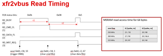
    I got some input from another team member more experienced with xrf2vbus, hopefully this is helpful!

    Regards,

    Nick

  • Hello Nick,

    thank you for your answer! I was on vacation and look into the behaviour the next days.

    Regards,

    Dominik

  • Hello Nick,

    yesterday I was abled to verify the behaviour of the timing diagram you provided. Therefore I have to admitt there was a little bug in the C-code i provided earier. The 256byte buffer where i wanted to save the status of the RD_BUSY bit was to big for the stack.

    One thing i was wondering about was, that the read is done when R18 has the value 0x5. Compared to the programming modell for a read access from the TRM rev.F (p.3168):

    Read:

    • Wait RD_BUSY = 0h

    • XOUT R18 (configure RD_AUTO/ RD_SIZE); R19 (RD_ADDR)

    Wait WR_BUSY = 0h OR RD_DATA_FL = 1h

    • XIN RD_DATA (Repeat if RD_AUTO is enabled and need new RD_DATA, must always check RD_DATA_FL before XIN RD_DATA)

    My suggestion would be to correct the highlighted line in the TRM of the AM64. (Maybe change it to: "Wait R18 =  0x05" ) To simply wait for bit 0 in R18 to be 0 didnt work in my tests.

    I will post my working PRU C-code on friday since I am short on time today.

    Regards,

    Dominik

  • The PRU program to verify the status of the xfr2vbus read device looks like this:

    #include <stdint.h>
    #include <stdbool.h>
    #include <stdio.h>
    
    #define RD_SIZE_POS 1
    #define RD_4_BYTES 0x0
    #define RD_32_BYTES 0x2
    #define RD_64_BYTES 0x3
    #define PRU_REG_WIDTH 32ULL
    
    #define WR_ID0 0x62
    #define RD_ID0 0x60
    
    #define RD_ADDR 19
    #define RD_BUSY 18
    #define RD_DATA 2
    
    #define WR_BUSY 20
    #define WR_DATA 2
    #define WR_ADDR 10
    
    #define NO_REMAPPING 0
    
    #define DDR_START_ADDRESS ((uint32_t)0x80000000)
    #define DDR_REGION_ADDRESS ((uint32_t)0xA6000000)
    
    /*
     * These structs (datagram_type) and (container_type) force the compiler to align data 64bit-wise.
     * This is necessary in order to use it with the xfr2vbus
     * accelerators
     *  */
    
    struct datagram_type{
        uint64_t r2and3; //data
        uint64_t r4and5; //data
        uint64_t r6and7; //data
        uint64_t r8and9; //data
        uint64_t r10and11; //addr
    };
    
    struct container_type{
        uint64_t r2and3; //data
        uint64_t r4and5; //data
        uint64_t r6and7; //data
        uint64_t r8and9; //data
      };
    
    typedef union package{
        struct datagram_type datagram;
        uint8_t bytes[sizeof(struct datagram_type)];
    }frame;
    
    typedef union package_wo_addr{
        struct container_type datagram;
        uint8_t bytes[sizeof(struct container_type)];
    }frame_wo_addr;
    
    /* global variables */
    
    frame data_2_send;
    frame dbg_2_send;
    frame_wo_addr data_2_read;
    
    /* test variable */
    
    #define TEST_BUF_SIZE 256
    uint8_t buf[TEST_BUF_SIZE] = {0}; /* Note for me: THIS BUFFER CANNOT BE DEFINED WITHIN THE MAIN SINCE THERE IS NOT ENOUGH SPACE ON THE STACK!!! */
    
    int main(void)
    {
        uint32_t write_busy_status = 1;
        uint32_t read_busy_status  = 1;
        int cnt = 0;
        uint64_t read_cmd = 0;
    
    
        for(int i = 0; i < TEST_BUF_SIZE; i++ ){
            buf[i] = 0xFF;
        }
    
        /* Wait RD_BUSY = 0h */
        while((read_busy_status & 1) == 1)
        {
            __xin(RD_ID0, RD_BUSY, NO_REMAPPING, read_busy_status);
        }
        /* XOUT R18 (configure RD_AUTO/ RD_SIZE); */
        read_cmd = (((uint64_t)DDR_REGION_ADDRESS) << PRU_REG_WIDTH) | (RD_32_BYTES << RD_SIZE_POS ); //upper 32 bit is addr + lower 32 bit is config
        __xout(RD_ID0, RD_BUSY, NO_REMAPPING, read_cmd );
    
        /* Wait WR_BUSY = 0h OR RD_DATA_FL = 1h */
        read_busy_status  = 1;
        while( ((read_busy_status & 0xF) != 0x05) && ( cnt < TEST_BUF_SIZE ) )
        {
            __xin(RD_ID0, RD_BUSY, NO_REMAPPING, read_busy_status);
            buf[cnt] = read_busy_status;
            __delay_cycles(5);         /* to prevent permanent polling of the status */
            cnt++;
        }
        /* XIN RD_DATA */
        __xin(RD_ID0, RD_DATA, NO_REMAPPING, data_2_read );
        /* end read procedure */
    
        /* modify data */
        for(int z = 0; z < 32; z++)
        {
            data_2_send.bytes[z] = data_2_read.bytes[z] + 1;
        }
    
        /* write procedure */
        write_busy_status = 1;
        while((write_busy_status & 1) == 1) /* wait for (xfr2vbus)wr_dev_0 to be ready */
        {
            __xin(WR_ID0, WR_BUSY, NO_REMAPPING, write_busy_status);
        }
        data_2_send.datagram.r10and11 = (DDR_REGION_ADDRESS);
        __xout(WR_ID0, WR_DATA, NO_REMAPPING, data_2_send );
    
        /*end write procedure*/
    
    
        /* Write the status of the RD_BUSY register (lower byte) to DDR_REGION_ADDRESS + offset (5*32 bytes) */
        for(int y = 0; y < 8; y++)  /* 256 bytes = 8 cycles of 32 byte writes */
        {
            write_busy_status = 1;
            while((write_busy_status & 1) == 1) /* wait for (xfr2vbus)wr_dev_0 to be ready */
            {
                __xin(WR_ID0, WR_BUSY, NO_REMAPPING, write_busy_status);
            }
            for(int z = 0; z < 32; z++) /* copy 32 bytes from buffer to the send frame */
            {
                dbg_2_send.bytes[z] = buf[ z + (y*32) ] ;
            }
            dbg_2_send.datagram.r10and11 = ( DDR_REGION_ADDRESS + (5+y) * 32 );
            __xout( WR_ID0, WR_DATA, NO_REMAPPING, dbg_2_send );
        }
    
        __halt();
    }

    This code reads 32 byte at the address defined in DDR_REGION_ADDRESS, adds +1 to every byte and writes them back to the same address.

    With an offset of a few bytes, it writes the status of R18 of the read accelerator until it has the value 0x5 in the lower byte.

    Seen from linux it looks like this:

    root@am64xx-evm:~# ./dma-heap-view | head -n 14
    00000000: 21 43 65 87 21 43 65 87 21 43 65 87 21 43 65 87 21 43 65 87 21 43 65 87 21 43 65 87 21 43 65 87
    00000020: 21 43 65 87 21 43 65 87 21 43 65 87 21 43 65 87 21 43 65 87 21 43 65 87 21 43 65 87 21 43 65 87
    00000040: 21 43 65 87 21 43 65 87 21 43 65 87 21 43 65 87 21 43 65 87 21 43 65 87 21 43 65 87 21 43 65 87
    ...
    
    root@am64xx-evm:~# echo pru/pru-dma-demo.out > /sys/class/remoteproc/remoteproc6/firmware
    root@am64xx-evm:~# echo start > /sys/class/remoteproc/remoteproc6/state
    root@am64xx-evm:~# echo stop > /sys/class/remoteproc/remoteproc6/state
    root@am64xx-evm:~# ./dma-heap-view | head -n 14
    00000000: 22 44 66 88 22 44 66 88 22 44 66 88 22 44 66 88 22 44 66 88 22 44 66 88 22 44 66 88 22 44 66 88
    00000020: 21 43 65 87 21 43 65 87 21 43 65 87 21 43 65 87 21 43 65 87 21 43 65 87 21 43 65 87 21 43 65 87
    00000040: 21 43 65 87 21 43 65 87 21 43 65 87 21 43 65 87 21 43 65 87 21 43 65 87 21 43 65 87 21 43 65 87
    00000060: 21 43 65 87 21 43 65 87 21 43 65 87 21 43 65 87 21 43 65 87 21 43 65 87 21 43 65 87 21 43 65 87
    00000080: 21 43 65 87 21 43 65 87 21 43 65 87 21 43 65 87 21 43 65 87 21 43 65 87 21 43 65 87 21 43 65 87
    000000A0: 0B 0B 0B 0B 08 05 FF FF FF FF FF FF FF FF FF FF FF FF FF FF FF FF FF FF FF FF FF FF FF FF FF FF
    000000C0: FF FF FF FF FF FF FF FF FF FF FF FF FF FF FF FF FF FF FF FF FF FF FF FF FF FF FF FF FF FF FF FF
    000000E0: FF FF FF FF FF FF FF FF FF FF FF FF FF FF FF FF FF FF FF FF FF FF FF FF FF FF FF FF FF FF FF FF
    00000100: FF FF FF FF FF FF FF FF FF FF FF FF FF FF FF FF FF FF FF FF FF FF FF FF FF FF FF FF FF FF FF FF
    00000120: FF FF FF FF FF FF FF FF FF FF FF FF FF FF FF FF FF FF FF FF FF FF FF FF FF FF FF FF FF FF FF FF
    00000140: FF FF FF FF FF FF FF FF FF FF FF FF FF FF FF FF FF FF FF FF FF FF FF FF FF FF FF FF FF FF FF FF
    00000160: FF FF FF FF FF FF FF FF FF FF FF FF FF FF FF FF FF FF FF FF FF FF FF FF FF FF FF FF FF FF FF FF
    00000180: FF FF FF FF FF FF FF FF FF FF FF FF FF FF FF FF FF FF FF FF FF FF FF FF FF FF FF FF FF FF FF FF
    

    The status switches after the read command from: 0x0b to 0x08 to 0x05 like your diagramm said.

    Maybe this code helps someone with beginning to use the xfr2vbus accelerators on the am64x.

    If you have further questions feel free to contact me, and thank you for your help Nick!

    Regards,

    Dominik