This thread has been locked.

If you have a related question, please click the "Ask a related question" button in the top right corner. The newly created question will be automatically linked to this question.

TMS320C6748: GROUPB 1.8V circuit short issue

Part Number: TMS320C6748

Hi team,

Here's an issue from the customer may need your help:

In mass production, some power pins on the EZCED4 groupb were found to be shorted (the short circuit behavior disappeared after the chip board was removed).

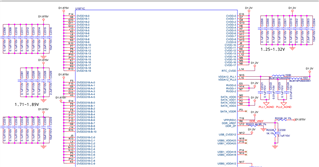
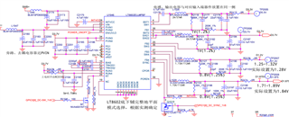
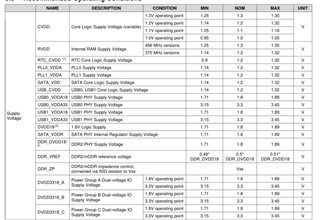
Measure the bottom pin of the BGA to verify that the power supply on the groupb is indeed shorted to the GND pin. The core uses 1.28V and the digital power uses 1.84V. The power-up sequence follows 1.28-V first up, 1.84-V second up and the power supply ripple is within 30 mV.

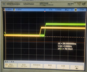
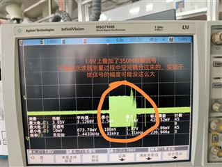
The DSP is used on the transceiver, so a 350 MHz RF signal is superimposed on the power rail in the transmit and receive state. At 4W emissions, this signal is tested with an oscilloscope with a large peak of 1VPP (the scope is tested with unlimited bandwidth, possibly spatial coupling effects measurements).

What is the possible cause of shorting the 1.84-V power network of the DSP? Is it possible for high frequency interference to damage the chip?

The following pins are shorted (the probability is around 5%-6% ):

Could you help check this case? Thanks.

Best Regards,

Cherry

  • Hello Cherry,

    Thank you for the query.

    I am not sure if we can analyze the issue with the above inputs. Let me review the inputs.

    If you have some additional details, that will help.

    In mass production, some power pins on the EZCED4 groupb were found to be shorted (the short circuit behavior disappeared after the chip board was removed).

    Could you help us understand the failure ratio.

    Can you confirm if the fixes specified in the errata as below are taken care.

    TMS320C6748 Fixed- and Floating-Point DSP (Revs 2.3, 2.1, 2.0, 1.1 & 1.0) (Rev. H)

    Regards,

    Sreenivasa

  • Hi Sreenivasa,

    Thanks for your support.

    Could you help us understand the failure ratio.

    About 17,18 of the more than 300 devices have a short circuit condition. The failure ratio is approximately 5%-6%.

    The circuits dvdd18 and dvdd1833_x use the same power source, both 1.84 V. The following is the supply network for the power section:

    The following power-up timing is measured for 1.28 V and 1.84 V: 

    Thanks and regards,

    Cherry

  • Hello Cherry, 

    Thank you for the inputs.

    Could you help us understand the failure ratio.

    About 17,18 of the more than 300 devices have a short circuit condition. The failure ratio is approximately 5%-6%.

    Could you provide some additional details on the failure phenomenon.

    Does this happen during the first power-up or after working for some time or if there is any other mode of failure.

    The following power-up timing is measured for 1.28 V and 1.84 V: 

    Any reason to have the voltages on the higher side.

    What is the power supply solution used?

    Regards,

    Sreenivasa

  • Hi Sreenivasa,

    Could you provide some additional details on the failure phenomenon.

    Most faults occur during operation and in the transmit state. Very few occur on first power up after DSP soldering is complete. 

    Any reason to have the voltages on the higher side.

    Could you help elaborate on this?

    What is the power supply solution used?

    One supply is 1.28V and the other is 1.8V. Once the 1.28V power-up is complete, the 1.8V power-up begins. The power supply scheme is as follows: 

    Also, with a 1.8V short circuit, the DSP can still be powered up (with higher currents), but some GPIO toggling is abnormal. 

    Thanks and regards,

    Cherry

  • Hello Cherry

    Thank you for the inputs.

    My question is why is the 1.2V set to 1.28V?

    Let me review the inputs and heck internally.

    Regarding failed units vs working units, do they have similar batch codes.

    Are these devices purchased from authorized distributor.

    Is this the first batch you are manufacturing these boards or have these board been manufactured previously without issue.

    Regards,

    Sreenivasa

  • Hello Cherry

    Would you be able to share the schematics snap shots you have above in a PDF format for me to check internally.

    Regards,

    Sreenivasa

  • Hello Cherry

    Most faults occur during operation and in the transmit state. Very few occur on first power up after DSP soldering is complete. 

    During operation - could you elaborate please. Is this failing in the factory or in the field etc.

    in the transmit state - could you elaborate please. 

    Regards,

    Sreenivasa

  • Hello Cherry

    I see that you mentioned this as the test condition

    a 350 MHz RF signal is superimposed on the power rail in the transmit and receive state

    Could you share a connection diagram. A handwritten should also be fine if you do not have one.

    Regards,

    Sreenivasa

  • Hi Sreenivasa,

    My question is why is the 1.2V set to 1.28V?

    The chip is 456MHz version, so it is set to 1.28V such that cvdd,rvdd RTC_cvdd requires only one power supply.

    Below is the recommended power supply for the manual, 1.28V should be in the range?

    Regarding failed units vs working units, do they have similar batch codes.

    Are these devices purchased from authorized distributor.

    The software version of the DSP is basically the same.

    The chip was purchased from an agent on TI's official website.

    Is this the first batch you are manufacturing these boards or have these board been manufactured previously without issue.

    800 units have been produced before without this issue. However, this time the customer outsourced to another manufacturer and found that there was a short circuit condition at 1.8 V (the circuit produced was adjusted, the pre-supply of 1.8V was given RF at 3.7V, and no other DSP peripherals were changed).

    Would you be able to share the schematics snap shots you have above in a PDF format for me to check internally.

    Please check private message regarding the schematic.

    Thanks and regards,

    Cherry

  • Hello Cherry

    Thank you for the inputs.

    I see that you mentioned this as the test condition

    a 350 MHz RF signal is superimposed on the power rail in the transmit and receive state

    Could you share a connection diagram. A handwritten should also be fine if you do not have one.

    Could you please elaborate the test condition.

    Regards,

    Sreenivasa

  • Hi Sreenivasa,

    During operation - could you elaborate please. Is this failing in the factory or in the field etc.

    in the transmit state - could you elaborate please. 

    During operation refers to damage to the device's power-on test function or aging during production on the production line. 

    a 350 MHz RF signal is superimposed on the power rail in the transmit and receive state

    Could you share a connection diagram. A handwritten should also be fine if you do not have one.

    The interference signal (350M carrier or modulation FSK encoding) superimposed on 1.8V is shown in the following figure: 

    (Chinses on the figure means “A 350M RF signal is superimposed on 1.8V. It may be spatially coupled during the measurement, and the magnitude of the disturbance signal may not be as large in reality”)

    Thanks and regards,

    Cherry

  • Hello Cherry

    Thank you for the inputs.

    The above is the scope capture. of the 1.8V supply and thank you for the picture. 

    The interference signal (350M carrier or modulation FSK encoding) superimposed on 1.8V is shown in the following figure: 

    I understand the signal being superimposed.Can you please help understand the coupling mechanism.

    Means how is the 350M getting coupled to the 1.8V. Would this be on all supply rails or only 1.8V.

    Regards,

    Sreenivasa

  • Hi Sreenivasa,

    Means how is the 350M getting coupled to the 1.8V. Would this be on all supply rails or only 1.8V.

    On all supply rails.

    One is that the high power emissions of the equipment are spatially coupled, affecting the scope measurements.
    The other part affects B+/3.7V through power supply conduction (these two supplies directly power the RF amplifier) and then conducts to 1.8V.

    If the scope measurement is within a 20M bandwidth limit, the ripple at 1.8V is within 50mV.

    Thanks and regards,

    Cherry

  • Hello Cherry

    Thank you for the inputs.

    800 units have been produced before without this issue.

    However, this time the customer outsourced to another manufacturer and found that there was a short circuit condition at 1.8 V (the circuit produced was adjusted, the pre-supply of 1.8V was given RF at 3.7V, and no other DSP peripherals were changed).

    You mentioned that the initial 800 from one of the manufacturer had no failures. I assume this is a correct assumption. 

    When the manufacturer was changed they are seeing failures.

    Based on the discussion internally, we believe the probable cause of failure could be the EOS that could be happening in the manufacturing due to the process change.

    I assume the process of sourcing/procuring the device did not change. I assume the required manufacturing precautions while handling the devices have been followed by the new manufacturer and audited by your customer.

    Regards,

    Sreenivasa

  • Hi Sreenivasa,

    As per the schematic, there's nothing special or wrong, right? 

    Thanks and regards,

    Cherry

  • Hello Cherry

    Thank you for checking.

    I have not looked at the schematics completely.

    I see the power solution used is different and i assume all the power supply normal operational requirements are tested.

    Have you considered adding additional filters on the supply rails, given that you expect high noise level to couple. the device would expect a stable DC supply.

    Regards,

    Sreenivasa

  • Hello Cherry

    Can you please read through the below thread and review the power supply implementation.

    (+) AM4372: Power-down sequence - Processors forum - Processors - TI E2E support forums

    Regards,

    Sreenivasa