This thread has been locked.

If you have a related question, please click the "Ask a related question" button in the top right corner. The newly created question will be automatically linked to this question.

TDA4AL-Q1: Unable to use MCAN15 on mcu2-1

Part Number: TDA4AL-Q1

Hell Ti ,

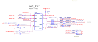
Configure can7 as follows,can7 can only receive a signal once, and after that, there will be no human signal or waveform. Could you please help confirm what can7 should be configured according to? thanks.  The following is the configuration of can7.
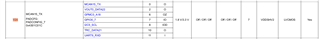
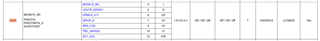
Current status:

Phenomenon: After being powered on, there was a data transmission signal, and then it disappeared;

We configure PINMUX related information in the code according to MCAN15;

MCAN15_ The voltage of the STB PIN pin has been lowered and entered the working mode, and the voltage has not been raised after entering the working mode;

  • #include <can_1.h>
    
    #define MCAN7_STB_PIN                   (0x24) /*CAN1*/
    #define MCU_MCAN1_STB_PIN               (0x19) /*CAN2*/
    
    #define MCU_MCAN0_ENABLE_PIN            (0x11)
    #define MCU_MCAN0_STBZ_PIN              (0x45)
    
    #define APP_MAIN_MCAN_DEF_INST0_INT0                (CSLR_R5FSS1_CORE1_INTR_MCAN15_MCANSS_MCAN_LVL_INT_0)
    #define APP_MAIN_MCAN_DEF_INST0_INT1                (CSLR_R5FSS1_CORE1_INTR_MCAN15_MCANSS_MCAN_LVL_INT_1)
    #define APP_MAIN_MCAN_DEF_INST0_TS_INT              (CSLR_R5FSS1_CORE1_INTR_MCAN15_MCANSS_EXT_TS_ROLLOVER_LVL_INT_0)
    
    #define APP_MAIN_MCAN_DEF_INST1_INT0                (CSLR_R5FSS1_CORE1_INTR_MCAN16_MCANSS_MCAN_LVL_INT_0)
    #define APP_MAIN_MCAN_DEF_INST1_INT1                (CSLR_R5FSS1_CORE1_INTR_MCAN16_MCANSS_MCAN_LVL_INT_1)
    #define APP_MAIN_MCAN_DEF_INST1_TS_INT              (CSLR_R5FSS1_CORE1_INTR_MCAN16_MCANSS_EXT_TS_ROLLOVER_LVL_INT_0)
    
    
    #define CAN_RX_TSK_STACK        (32U * 1024U)
    #define CAN_TX_TSK_STACK        (32U * 1024U)
    
    static volatile uint32_t gMcanIsrIntr0Flag = 1U, gMcanIsrIntr0Flag_lpbk = 1U;
    static volatile uint32_t gMcanIsrIntr1Flag = 1U, gMcanIsrIntr1Flag_lpbk = 1U;
    static uint32_t          gMcanAppdataSize[16] =
    {0, 1, 2, 3, 4, 5, 6, 7, 8, 12, 16, 20, 24, 32, 48, 64};
    
    static uint32_t gMcanModAddr, gMcanModAddr_lpbk;
    
    static uint8_t  gCanRxTskStack[CAN_RX_TSK_STACK]
    __attribute__ ((aligned(8192)));
    
    static uint8_t  gCanTxTskStack[CAN_TX_TSK_STACK]
    __attribute__ ((aligned(8192)));
    
    
    static void App_mcanIntr0ISR(uintptr_t arg)
    {
        uint32_t intrStatus;
    
        intrStatus = MCAN_getIntrStatus(gMcanModAddr);
        MCAN_clearIntrStatus(gMcanModAddr, intrStatus);
        if (MCAN_INTR_SRC_TRANS_COMPLETE ==
            (intrStatus & MCAN_INTR_SRC_TRANS_COMPLETE))
        {
            gMcanIsrIntr0Flag = 0U;
        }
    
        if (MCAN_INTR_SRC_DEDICATED_RX_BUFF_MSG ==
            (intrStatus & MCAN_INTR_SRC_DEDICATED_RX_BUFF_MSG))
        {
            gMcanIsrIntr1Flag = 0U;
        }
    
        if(MCAN_INTR_SRC_RX_FIFO0_NEW_MSG ==
            (intrStatus & MCAN_INTR_SRC_RX_FIFO0_NEW_MSG))
        {
            gMcanIsrIntr1Flag = 0U;
        }
    
    }
    
    static void App_mcanIntr1ISR(uintptr_t arg)
    {
        uint32_t intrStatus;
    
        intrStatus = MCAN_getIntrStatus(gMcanModAddr);
        MCAN_clearIntrStatus(gMcanModAddr, intrStatus);
    
        if (MCAN_INTR_SRC_DEDICATED_RX_BUFF_MSG ==
            (intrStatus & MCAN_INTR_SRC_DEDICATED_RX_BUFF_MSG))
        {
            gMcanIsrIntr1Flag = 0U;
        }
    
        if(MCAN_INTR_SRC_RX_FIFO0_NEW_MSG ==
            (intrStatus & MCAN_INTR_SRC_RX_FIFO0_NEW_MSG))
        {
            gMcanIsrIntr1Flag = 0U;
        }
    }
    
    static void App_mcanTSIntrISR(uintptr_t arg)
    {
        CAN_PRINTF_INFO("Time Stamp overflow happened.");
    }
    
    
    static int32_t App_mcanRegisterIsr(uint32_t mcanInstAddr)
    {
        int32_t configStatus = STW_SOK;
    
        /* Running Code from Main R5 */
        /* Main MCAN Default Tx Inst  */
        configStatus =  App_mcanRegisterInterrupt(APP_MAIN_MCAN_DEF_INST0_INT0, &App_mcanIntr0ISR);
        configStatus += App_mcanRegisterInterrupt(APP_MAIN_MCAN_DEF_INST0_INT1, &App_mcanIntr1ISR);
        configStatus += App_mcanRegisterInterrupt(APP_MAIN_MCAN_DEF_INST0_TS_INT, &App_mcanTSIntrISR);
        /* Main MCAN Default Rx Inst*/
        configStatus =  App_mcanRegisterInterrupt(APP_MAIN_MCAN_DEF_INST1_INT0, &App_mcanIntr0ISR);
        configStatus += App_mcanRegisterInterrupt(APP_MAIN_MCAN_DEF_INST1_INT1, &App_mcanIntr1ISR);
        configStatus += App_mcanRegisterInterrupt(APP_MAIN_MCAN_DEF_INST1_TS_INT, &App_mcanTSIntrISR);
    
        if(STW_SOK != configStatus)
        {
            CAN_PRINTF_INFO("CrossBar/Interrupt Configuration failed.\n");
        }
        else
        {
            CAN_PRINTF_INFO("CrossBar/Interrupt Configuration done.\n");
        }
    
        return configStatus;
    }


    static void APP_mcanRx(void)
    {
        uint32_t             loopCnt    = 1U, chkCnt = 0U;
        int32_t              testStatus = CSL_PASS;
        MCAN_RxBufElement    rxMsg;
        MCAN_RxNewDataStatus newDataStatus;
        MCAN_ErrCntStatus    errCounter;
    
        /* Enable Interrupts */
        MCAN_enableIntr(gMcanModAddr, MCAN_INTR_MASK_ALL, (uint32_t)TRUE);
        MCAN_enableIntr(gMcanModAddr,
                        MCAN_INTR_SRC_RES_ADDR_ACCESS, (uint32_t)FALSE);
        /* Select Interrupt Line */
        MCAN_selectIntrLine(gMcanModAddr,
                            MCAN_INTR_MASK_ALL,
                            MCAN_INTR_LINE_NUM_1);
        /* Enable Interrupt Line */
        MCAN_enableIntrLine(gMcanModAddr,
                            MCAN_INTR_LINE_NUM_1,
                            1U);
    
        while (gMcanIsrIntr1Flag)
        {
            appLogWaitMsecs(1U);
        }
        gMcanIsrIntr1Flag = 1U;
        /* Checking for Errors */
        MCAN_getErrCounters(gMcanModAddr, &errCounter);
        if ((0U == errCounter.recErrCnt) &&
            (0U == errCounter.canErrLogCnt))
        {
            MCAN_getNewDataStatus(gMcanModAddr, &newDataStatus);
            MCAN_clearNewDataStatus(gMcanModAddr, &newDataStatus);
            MCAN_readMsgRam(gMcanModAddr,
                MCAN_MEM_TYPE_FIFO,
                0U,
                0U,
                &rxMsg);
        }
        else
        {
            testStatus = CSL_EFAIL;
        }
    
        CAN_PRINTF_INFO("Received last message with following details: ");
        App_mcanPrintRxMsg(&rxMsg);
        if (CSL_EFAIL == testStatus)
        {
            CAN_PRINTF_INFO("Rx  FAILED...");
        }
        else
        {
            CAN_PRINTF_DEBUG("Rx  PASSED...");
        }
    }
    
    
    static void MCanRxTaskFunc(void* arg0, void* arg1)
    {
        CAN_PRINTF_INFO("Create rx task success");
        while(1)
        {
            APP_mcanRx();
        }
    }
    
    static void APP_mcanTx(MCAN_TxBufElement *txMsg)
    {
        int32_t  testStatus = CSL_PASS;
        uint32_t loopCnt      = 1U;
        MCAN_ProtocolStatus protStatus;
    
        /* Enable Interrupts */
        MCAN_enableIntr(gMcanModAddr, MCAN_INTR_MASK_ALL, (uint32_t)TRUE);
        MCAN_enableIntr(gMcanModAddr,
                        MCAN_INTR_SRC_RES_ADDR_ACCESS, (uint32_t)FALSE);
        /* Select Interrupt Line */
        MCAN_selectIntrLine(gMcanModAddr,
                            MCAN_INTR_MASK_ALL,
                            MCAN_INTR_LINE_NUM_0);
        /* Enable Interrupt Line */
        MCAN_enableIntrLine(gMcanModAddr,
                            MCAN_INTR_LINE_NUM_0,
                            1U);
        /* Enable Transmission interrupt */
        testStatus = MCAN_txBufTransIntrEnable(gMcanModAddr,
                                               1U,
                                               (uint32_t)TRUE);
    
        if (CSL_PASS != testStatus)
        {
            CAN_PRINTF_INFO("Error in enabling buffer Transmit interrupt...");
        }
        else
        {
            {
                /* Write message to Msg RAM */
                MCAN_writeMsgRam(gMcanModAddr,
                    MCAN_MEM_TYPE_BUF,
                    1U,
                    txMsg);
                /* Add request for transmission */
                testStatus = MCAN_txBufAddReq(gMcanModAddr, 1U);
                if (CSL_PASS != testStatus)
                {
                    CAN_PRINTF_INFO("\nError in Adding Transmission Request...");
                }
                {
                    appLogWaitMsecs(1U);
                }
                gMcanIsrIntr0Flag = 1U;
                MCAN_getProtocolStatus(gMcanModAddr, &protStatus);
                /* Checking for Errors */
                if (((MCAN_ERR_CODE_NO_ERROR == protStatus.lastErrCode) ||
                        (MCAN_ERR_CODE_NO_CHANGE == protStatus.lastErrCode)) &&
                    ((MCAN_ERR_CODE_NO_ERROR == protStatus.dlec) ||
                     (MCAN_ERR_CODE_NO_CHANGE == protStatus.dlec)) &&
                    (0U == protStatus.pxe))
                {
                    CAN_PRINTF_DEBUG(
                        "Message successfully transferred with payload Bytes:%d ",
                        gMcanAppdataSize[txMsg->dlc]);
                }
                else
                {
                    CAN_PRINTF_INFO(
                        "Error in transmission with payload Bytes:%d \n",
                        gMcanAppdataSize[txMsg->d7c]);
    
                    CAN_PRINTF_ERROR("lastErrCode = 0x%x,dlec = 0x%x,pxe = %d",protStatus.lastErrCode,protStatus.dlec,protStatus.pxe);
                    testStatus = CSL_EFAIL;
                }
            }
        }
    
        if (CSL_EFAIL == testStatus)
        {
            CAN_PRINTF_INFO("Tx Test FAILED...");
        }
        else
        {
            CAN_PRINTF_DEBUG("Tx Test PASSED...");
        }
    }
    
    static void MCanTxTaskFunc(void* arg0, void* arg1)
    {
        CAN_PRINTF_INFO("Create tx task success");
        static MCAN_TxBufElement          txMsg;
        uint32_t                   loopCnt = 0U;
    
        /* Initialize message to transmit */
        txMsg.id  = can_fd_id_transform_message_id(0x99);
        txMsg.rtr = 0U;
        txMsg.xtd = 0U;
        txMsg.esi = 0U;
        txMsg.dlc = 0x2U;
        txMsg.brs = 1U;
        txMsg.fdf = 1U;
        txMsg.efc = 1U;
        txMsg.mm  = 0xAAU;
        txMsg.data[0] = 20;
        txMsg.data[1] = 23;
        while(1)
        {
            APP_mcanTx(&txMsg);
            appLogWaitMsecs(1000u);
        }
    }
    
    void padConfig_prcmEnable()
    {
        GPIOSetDirMode_v0(CSL_WKUP_GPIO0_BASE, MCAN7_STB_PIN, GPIO_DIRECTION_OUTPUT);
        GPIOPinWrite_v0(CSL_WKUP_GPIO0_BASE, MCAN7_STB_PIN, GPIO_PIN_LOW);
    }
    
    void mcu2_1_can7_main(void)
    {
        TaskP_Handle canRxTask;
        TaskP_Params canRxTaskParams;
        TaskP_Handle canTxTask;
        TaskP_Params canTxTaskParams;
    
        int32_t configStatus = CSL_PASS;
        /* Used to test the selection of different CAN */
        uint32_t mcan_num;
    
        appLogWaitMsecs(20u);
    
        padConfig_prcmEnable();
    
        /* 修改为当前can的地址*/
        gMcanModAddr = CSL_MCAN15_MSGMEM_RAM_BASE;
    
        configStatus = App_mcanRegisterIsr(gMcanModAddr);
        App_mcanConfig(gMcanModAddr,FALSE);
    
        TaskP_Params_init(&canRxTaskParams);
        canRxTaskParams.priority     = 2;
        canRxTaskParams.stack        = gCanRxTskStack;
        canRxTaskParams.stacksize    = sizeof (gCanRxTskStack);
        canRxTask = TaskP_create(&MCanRxTaskFunc, &canRxTaskParams);
    
        TaskP_Params_init(&canTxTaskParams);
        canTxTaskParams.priority     = 2;
        canTxTaskParams.stack        = gCanTxTskStack;
        canTxTaskParams.stacksize    = sizeof (gCanTxTskStack);
        canTxTask = TaskP_create(&MCanTxTaskFunc, &canTxTaskParams);
    
    }

  • /**
    * Note: This file was auto-generated by TI PinMux on 10/24/2021 at 3:31:41 AM.
    *
    * \file  J721S2_pinmux_data.c
    *
    * \brief  This file contains the pin mux configurations for the boards.
    *         These are prepared based on how the peripherals are extended on
    *         the boards.
    *
    * \copyright Copyright (CU) 2021 Texas Instruments Incorporated -
    *             http://www.ti.com/
    */
    
    /* ========================================================================== */
    /*                             Include Files                                  */
    /* ========================================================================== */
    
    #include "J721S2_pinmux.h"
    
    /** Peripheral Pin Configurations */
    
    
    static pinmuxPerCfg_t gCpsw2g0PinCfg[] =
    {
    #if 0
        /* MyCPSW2G0 -> MDIO0_MDC -> T28 */
        {
            PIN_MCASP1_AXR0, PIN_MODE(6) | \
            ((PIN_PULL_DISABLE | PIN_INPUT_ENABLE) & (~PIN_PULL_DIRECTION))
        },
        /* MyCPSW2G0 -> MDIO0_MDIO -> V28 */
        {
            PIN_MCASP1_AFSX, PIN_MODE(6) | \
            ((PIN_PULL_DISABLE | PIN_INPUT_ENABLE) & (~PIN_PULL_DIRECTION))
        },
    #endif
        /* MyCPSW2G0 -> RGMII1_RD0 -> AA24 */
        {
            PIN_MCASP1_ACLKX, PIN_MODE(6) | \
            ((PIN_PULL_DISABLE | PIN_INPUT_ENABLE) & (~PIN_PULL_DIRECTION))
        },
        /* MyCPSW2G0 -> RGMII1_RD1 -> AB25 */
        {
            PIN_MCASP0_AXR12, PIN_MODE(6) | \
            ((PIN_PULL_DISABLE | PIN_INPUT_ENABLE) & (~PIN_PULL_DIRECTION))
        },
        /* MyCPSW2G0 -> RGMII1_RD2 -> T23 */
        {
            PIN_MCASP0_AXR13, PIN_MODE(6) | \
            ((PIN_PULL_DISABLE | PIN_INPUT_ENABLE) & (~PIN_PULL_DIRECTION))
        },
        /* MyCPSW2G0 -> RGMII1_RD3 -> U24 */
        {
            PIN_MCASP0_AXR14, PIN_MODE(6) | \
            ((PIN_PULL_DISABLE | PIN_INPUT_ENABLE) & (~PIN_PULL_DIRECTION))
        },
        /* MyCPSW2G0 -> RGMII1_RXC -> AD26 */
        {
            PIN_MCASP1_AXR3, PIN_MODE(6) | \
            ((PIN_PULL_DISABLE | PIN_INPUT_ENABLE) & (~PIN_PULL_DIRECTION))
        },
        /* MyCPSW2G0 -> RGMII1_RX_CTL -> AC25 */
        {
            PIN_MCASP0_AXR15, PIN_MODE(6) | \
            ((PIN_PULL_DISABLE | PIN_INPUT_ENABLE) & (~PIN_PULL_DIRECTION))
        },
        /* MyCPSW2G0 -> RGMII1_TD0 -> T25 */
        {
            PIN_MCASP0_AXR7, PIN_MODE(6) | \
            ((PIN_PULL_DISABLE | PIN_INPUT_ENABLE) & (~PIN_PULL_DIRECTION))
        },
        /* MyCPSW2G0 -> RGMII1_TD1 -> W24 */
        {
            PIN_MCASP0_AXR8, PIN_MODE(6) | \
            ((PIN_PULL_DISABLE | PIN_INPUT_ENABLE) & (~PIN_PULL_DIRECTION))
        },
        /* MyCPSW2G0 -> RGMII1_TD2 -> AA25 */
        {
            PIN_MCASP0_AXR9, PIN_MODE(6) | \
            ((PIN_PULL_DISABLE | PIN_INPUT_ENABLE) & (~PIN_PULL_DIRECTION))
        },
        /* MyCPSW2G0 -> RGMII1_TD3 -> V25 */
        {
            PIN_MCASP0_AXR10, PIN_MODE(6) | \
            ((PIN_PULL_DISABLE | PIN_INPUT_ENABLE) & (~PIN_PULL_DIRECTION))
        },
        /* MyCPSW2G0 -> RGMII1_TXC -> U25 */
        {
            PIN_MCASP1_AXR4, PIN_MODE(6) | \
            ((PIN_PULL_DISABLE | PIN_INPUT_ENABLE) & (~PIN_PULL_DIRECTION))
        },
        /* MyCPSW2G0 -> RGMII1_TX_CTL -> T24 */
        {
            PIN_MCASP0_AXR11, PIN_MODE(6) | \
            ((PIN_PULL_DISABLE | PIN_INPUT_ENABLE) & (~PIN_PULL_DIRECTION))
        },
        {PINMUX_END}
    };
    
    static pinmuxModuleCfg_t gCpsw2gPinCfg[] =
    {
        {0, TRUE, gCpsw2g0PinCfg},
        {PINMUX_END}
    };
    
    
    static pinmuxPerCfg_t gGpio0PinCfg[] =
    {
        /* MyGPIO0 -> GPIO0_3 -> AE28 */
        {
            PIN_MCAN13_TX, PIN_MODE(7) | \
            ((PIN_PULL_DISABLE | PIN_INPUT_ENABLE) & (~PIN_PULL_DIRECTION))
        },
        /* MyGPIO0 -> GPIO0_8 -> AA23 */
        {
            PIN_MCAN15_RX, PIN_MODE(0) | \
            ((PIN_PULL_DISABLE | PIN_INPUT_ENABLE) & (~PIN_PULL_DIRECTION))
        },
        /* MyGPIO0 -> GPIO0_11 -> V23 */
        {
            PIN_GPIO0_11, PIN_MODE(7) | \
            ((PIN_PULL_DISABLE | PIN_INPUT_ENABLE) & (~PIN_PULL_DIRECTION))
        },
        /* MyGPIO0 -> GPIO0_13 -> AD24 */
        {
            PIN_PMIC_WAKE0, PIN_MODE(7) | \
            ((PIN_PULL_DISABLE | PIN_INPUT_ENABLE) & (~PIN_PULL_DIRECTION))
        },
        /* MyGPIO0 -> GPIO0_18 -> AB27 */
        {
            PIN_MCASP0_AXR2, PIN_MODE(7) | \
            ((PIN_PULL_DISABLE | PIN_INPUT_ENABLE) & (~PIN_PULL_DIRECTION))
        },
        /* MyGPIO0 -> GPIO0_23 -> AA26 */
        {
            PIN_MCASP2_AXR0, PIN_MODE(7) | \
            ((PIN_PULL_DISABLE | PIN_INPUT_ENABLE) & (~PIN_PULL_DIRECTION))
        },
    #if 0 //change can0
        /* MyGPIO0 -> GPIO0_26 -> U28 */
        {
            PIN_MCAN0_RX, PIN_MODE(7) | \
            ((PIN_PULL_DISABLE | PIN_INPUT_ENABLE) & (~PIN_PULL_DIRECTION))
        },
    #endif
        /* MyGPIO0 -> GPIO0_28 -> R27 */
        {
            PIN_MCAN1_RX, PIN_MODE(7) | \
            ((PIN_PULL_DISABLE | PIN_INPUT_ENABLE) & (~PIN_PULL_DIRECTION))
        },
        /* MyGPIO0 -> GPIO0_51 -> AE27 */
        {
            PIN_SPI0_CS0, PIN_MODE(7) | \
            ((PIN_PULL_DISABLE | PIN_INPUT_ENABLE) & (~PIN_PULL_DIRECTION))
        },
        {PINMUX_END}
    };
    
    static pinmuxModuleCfg_t gGpioPinCfg[] =
    {
        {0, TRUE, gGpio0PinCfg},
        {PINMUX_END}
    };
    
    
    static pinmuxPerCfg_t gI2c0PinCfg[] =
    {
        /* MyI2C0 -> I2C0_SCL -> AH25 */
        {
            PIN_I2C0_SCL, PIN_MODE(0) | \
            ((PIN_PULL_DISABLE | PIN_INPUT_ENABLE) & (~PIN_PULL_DIRECTION))
        },
        /* MyI2C0 -> I2C0_SDA -> AE24 */
        {
            PIN_I2C0_SDA, PIN_MODE(0) | \
            ((PIN_PULL_DISABLE | PIN_INPUT_ENABLE) & (~PIN_PULL_DIRECTION))
        },
        {PINMUX_END}
    };
    
    static pinmuxPerCfg_t gI2c1PinCfg[] =
    {
        /* MyI2C1 -> I2C1_SCL -> AB26 */
        {
            PIN_ECAP0_IN_APWM_OUT, PIN_MODE(13) | \
            ((PIN_PULL_DISABLE | PIN_INPUT_ENABLE) & (~PIN_PULL_DIRECTION))
        },
        /* MyI2C1 -> I2C1_SDA -> AD28 */
        {
            PIN_EXT_REFCLK1, PIN_MODE(13) | \
            ((PIN_PULL_DISABLE | PIN_INPUT_ENABLE) & (~PIN_PULL_DIRECTION))
        },
        {PINMUX_END}
    };
    
    static pinmuxPerCfg_t gI2c3PinCfg[] =
    {
    #if 0 //change can
        /* MyI2C3 -> I2C3_SCL -> W28 */
        {
            PIN_MCAN0_TX, PIN_MODE(13) | \
            ((PIN_PULL_DISABLE | PIN_INPUT_ENABLE) & (~PIN_PULL_DIRECTION))
        },
    #endif
        /* MyI2C3 -> I2C3_SDA -> AC27 */
        {
            PIN_MCASP2_AXR1, PIN_MODE(13) | \
            ((PIN_PULL_DISABLE | PIN_INPUT_ENABLE) & (~PIN_PULL_DIRECTION))
        },
    
        {PINMUX_END}
    };
    
    static pinmuxPerCfg_t gI2c4PinCfg[] =
    {
        /* MyI2C4 -> I2C4_SCL -> AD25 */
        {
            PIN_MCAN14_TX, PIN_MODE(8) | \
            ((PIN_PULL_DISABLE | PIN_INPUT_ENABLE) & (~PIN_PULL_DIRECTION))
        },
        /* MyI2C4 -> I2C4_SDA -> AF28 */
        {
            PIN_MCAN13_RX, PIN_MODE(8) | \
            ((PIN_PULL_DISABLE | PIN_INPUT_ENABLE) & (~PIN_PULL_DIRECTION))
        },
        {PINMUX_END}
    };
    
    static pinmuxPerCfg_t gI2c5PinCfg[] =
    {
        /* MyI2C5 -> I2C5_SCL -> Y24 */
        {
            PIN_MCAN15_TX, PIN_MODE(0) | \
            ((PIN_PULL_DISABLE | PIN_INPUT_ENABLE) & (~PIN_PULL_DIRECTION))
        },
        /* MyI2C5 -> I2C5_SDA -> W23 */
        {
            PIN_MCAN14_RX, PIN_MODE(8) | \
            ((PIN_PULL_DISABLE | PIN_INPUT_ENABLE) & (~PIN_PULL_DIRECTION))
        },
        {PINMUX_END}
    };
    
    static pinmuxModuleCfg_t gI2cPinCfg[] =
    {
        {0, TRUE, gI2c0PinCfg},
        {1, TRUE, gI2c1PinCfg},
        {3, TRUE, gI2c3PinCfg},
        {4, TRUE, gI2c4PinCfg},
        {5, TRUE, gI2c5PinCfg},
        {PINMUX_END}
    };
    
    
    static pinmuxPerCfg_t gMcan6PinCfg[] =
    {
        /* MyMCAN16 -> MCAN16_RX -> AB24 */
        {
            PIN_MCAN16_RX, PIN_MODE(0) | \
            ((PIN_PULL_DISABLE | PIN_INPUT_ENABLE) & (~PIN_PULL_DIRECTION))
        },
        /* MyMCAN16 -> MCAN16_TX -> Y28 */
        {
            PIN_MCAN16_TX, PIN_MODE(0) | \
            ((PIN_PULL_DISABLE | PIN_INPUT_ENABLE) & (~PIN_PULL_DIRECTION))
        },
        {PINMUX_END}
    };
    
    static pinmuxPerCfg_t gMcan3PinCfg[] =
    {
        /* MyMCAN3 -> MCAN3_RX -> U26 */
        {
            PIN_MCASP0_AXR4, PIN_MODE(0) | \
            ((PIN_PULL_DISABLE | PIN_INPUT_ENABLE) & (~PIN_PULL_DIRECTION))
        },
        /* MyMCAN3 -> MCAN3_TX -> T27 */
        {
            PIN_MCASP0_AXR3, PIN_MODE(0) | \
            ((PIN_PULL_DISABLE | PIN_INPUT_ENABLE) & (~PIN_PULL_DIRECTION))
        },
        {PINMUX_END}
    };
    
    static pinmuxPerCfg_t gMcan5PinCfg[] =
    {
        /* MyMCAN5 -> MCAN5_RX -> U27 */
        {
            PIN_MCASP0_AFSX, PIN_MODE(0) | \
            ((PIN_PULL_DISABLE | PIN_INPUT_ENABLE) & (~PIN_PULL_DIRECTION))
        },
        /* MyMCAN5 -> MCAN5_TX -> AB28 */
        {
            PIN_MCASP0_ACLKX, PIN_MODE(0) | \
            ((PIN_PULL_DISABLE | PIN_INPUT_ENABLE) & (~PIN_PULL_DIRECTION))
        },
        {PINMUX_END}
    };
    
    static pinmuxPerCfg_t gMcan4PinCfg[] =
    {
        /* MyMCAN4 -> MCAN4_RX -> AD27 */
        {
            PIN_MCASP0_AXR6, PIN_MODE(0) | \
            ((PIN_PULL_DISABLE | PIN_INPUT_ENABLE) & (~PIN_PULL_DIRECTION))
        },
        /* MyMCAN4 -> MCAN4_TX -> AA28 */
        {
            PIN_MCASP0_AXR5, PIN_MODE(0) | \
            ((PIN_PULL_DISABLE | PIN_INPUT_ENABLE) & (~PIN_PULL_DIRECTION))
        },
        {PINMUX_END}
    };
    
    static pinmuxPerCfg_t gMcan0PinCfg[] =
    {
        /* MyMCAN0 -> MCAN0_TX -> W28 */
        {
            PIN_MCAN0_TX, PIN_MODE(0) | \
            ((PIN_PULL_DISABLE | PIN_INPUT_ENABLE) & (~PIN_PULL_DIRECTION))
        },
        /* MyMCAN0 -> MCAN0_RX -> U28 */
        {
            PIN_MCAN0_RX, PIN_MODE(0) | \
            ((PIN_PULL_DISABLE | PIN_INPUT_ENABLE) & (~PIN_PULL_DIRECTION))
        },
    };
    
    static pinmuxModuleCfg_t gMcanPinCfg[] =
    {
        {6, TRUE, gMcan6PinCfg},
        {3, TRUE, gMcan3PinCfg},
        {5, TRUE, gMcan5PinCfg},
        {4, TRUE, gMcan4PinCfg},
        {0, TRUE, gMcan0PinCfg},
        {PINMUX_END}
    };
    
    
    static pinmuxPerCfg_t gMcu_adc0PinCfg[] =
    {
        /* MyMCU_ADC0 -> MCU_ADC0_AIN0 -> L25 */
        {
            PIN_MCU_ADC0_AIN0, PIN_MODE(0) | \
            ((PIN_PULL_DISABLE | PIN_INPUT_ENABLE) & (~PIN_PULL_DIRECTION))
        },
        /* MyMCU_ADC0 -> MCU_ADC0_AIN1 -> K25 */
        {
            PIN_MCU_ADC0_AIN1, PIN_MODE(0) | \
            ((PIN_PULL_DISABLE | PIN_INPUT_ENABLE) & (~PIN_PULL_DIRECTION))
        },
        /* MyMCU_ADC0 -> MCU_ADC0_AIN2 -> M24 */
        {
            PIN_MCU_ADC0_AIN2, PIN_MODE(0) | \
            ((PIN_PULL_DISABLE | PIN_INPUT_ENABLE) & (~PIN_PULL_DIRECTION))
        },
        /* MyMCU_ADC0 -> MCU_ADC0_AIN3 -> L24 */
        {
            PIN_MCU_ADC0_AIN3, PIN_MODE(0) | \
            ((PIN_PULL_DISABLE | PIN_INPUT_ENABLE) & (~PIN_PULL_DIRECTION))
        },
        /* MyMCU_ADC0 -> MCU_ADC0_AIN4 -> L27 */
        {
            PIN_MCU_ADC0_AIN4, PIN_MODE(0) | \
            ((PIN_PULL_DISABLE | PIN_INPUT_ENABLE) & (~PIN_PULL_DIRECTION))
        },
        /* MyMCU_ADC0 -> MCU_ADC0_AIN5 -> K24 */
        {
            PIN_MCU_ADC0_AIN5, PIN_MODE(0) | \
            ((PIN_PULL_DISABLE | PIN_INPUT_ENABLE) & (~PIN_PULL_DIRECTION))
        },
        /* MyMCU_ADC0 -> MCU_ADC0_AIN6 -> M27 */
        {
            PIN_MCU_ADC0_AIN6, PIN_MODE(0) | \
            ((PIN_PULL_DISABLE | PIN_INPUT_ENABLE) & (~PIN_PULL_DIRECTION))
        },
        /* MyMCU_ADC0 -> MCU_ADC0_AIN7 -> M26 */
        {
            PIN_MCU_ADC0_AIN7, PIN_MODE(0) | \
            ((PIN_PULL_DISABLE | PIN_INPUT_ENABLE) & (~PIN_PULL_DIRECTION))
        },
        {PINMUX_END}
    };
    
    static pinmuxPerCfg_t gMcu_adc1PinCfg[] =
    {
        /* MyMCU_ADC1 -> MCU_ADC1_AIN0 -> P25 */
        {
            PIN_MCU_ADC1_AIN0, PIN_MODE(0) | \
            ((PIN_PULL_DISABLE | PIN_INPUT_ENABLE) & (~PIN_PULL_DIRECTION))
        },
        /* MyMCU_ADC1 -> MCU_ADC1_AIN1 -> R25 */
        {
            PIN_MCU_ADC1_AIN1, PIN_MODE(0) | \
            ((PIN_PULL_DISABLE | PIN_INPUT_ENABLE) & (~PIN_PULL_DIRECTION))
        },
        /* MyMCU_ADC1 -> MCU_ADC1_AIN2 -> P28 */
        {
            PIN_MCU_ADC1_AIN2, PIN_MODE(0) | \
            ((PIN_PULL_DISABLE | PIN_INPUT_ENABLE) & (~PIN_PULL_DIRECTION))
        },
        /* MyMCU_ADC1 -> MCU_ADC1_AIN3 -> P27 */
        {
            PIN_MCU_ADC1_AIN3, PIN_MODE(0) | \
            ((PIN_PULL_DISABLE | PIN_INPUT_ENABLE) & (~PIN_PULL_DIRECTION))
        },
        /* MyMCU_ADC1 -> MCU_ADC1_AIN4 -> N25 */
        {
            PIN_MCU_ADC1_AIN4, PIN_MODE(0) | \
            ((PIN_PULL_DISABLE | PIN_INPUT_ENABLE) & (~PIN_PULL_DIRECTION))
        },
        /* MyMCU_ADC1 -> MCU_ADC1_AIN5 -> P26 */
        {
            PIN_MCU_ADC1_AIN5, PIN_MODE(0) | \
            ((PIN_PULL_DISABLE | PIN_INPUT_ENABLE) & (~PIN_PULL_DIRECTION))
        },
        /* MyMCU_ADC1 -> MCU_ADC1_AIN6 -> N26 */
        {
            PIN_MCU_ADC1_AIN6, PIN_MODE(0) | \
            ((PIN_PULL_DISABLE | PIN_INPUT_ENABLE) & (~PIN_PULL_DIRECTION))
        },
        /* MyMCU_ADC1 -> MCU_ADC1_AIN7 -> N27 */
        {
            PIN_MCU_ADC1_AIN7, PIN_MODE(0) | \
            ((PIN_PULL_DISABLE | PIN_INPUT_ENABLE) & (~PIN_PULL_DIRECTION))
        },
        {PINMUX_END}
    };
    
    static pinmuxModuleCfg_t gMcu_adcPinCfg[] =
    {
        {0, TRUE, gMcu_adc0PinCfg},
        {1, TRUE, gMcu_adc1PinCfg},
        {PINMUX_END}
    };
    
    
    static pinmuxPerCfg_t gMcu_cpsw2g0PinCfg[] =
    {
        /* MyMCU_CPSW2G0 -> MCU_RGMII1_RD0 -> B22 */
        {
            PIN_MCU_RGMII1_RD0, PIN_MODE(0) | \
            ((PIN_PULL_DISABLE | PIN_INPUT_ENABLE) & (~PIN_PULL_DIRECTION))
        },
        /* MyMCU_CPSW2G0 -> MCU_RGMII1_RD1 -> B21 */
        {
            PIN_MCU_RGMII1_RD1, PIN_MODE(0) | \
            ((PIN_PULL_DISABLE | PIN_INPUT_ENABLE) & (~PIN_PULL_DIRECTION))
        },
        /* MyMCU_CPSW2G0 -> MCU_RGMII1_RD2 -> C22 */
        {
            PIN_MCU_RGMII1_RD2, PIN_MODE(0) | \
            ((PIN_PULL_DISABLE | PIN_INPUT_ENABLE) & (~PIN_PULL_DIRECTION))
        },
        /* MyMCU_CPSW2G0 -> MCU_RGMII1_RD3 -> D23 */
        {
            PIN_MCU_RGMII1_RD3, PIN_MODE(0) | \
            ((PIN_PULL_DISABLE | PIN_INPUT_ENABLE) & (~PIN_PULL_DIRECTION))
        },
        /* MyMCU_CPSW2G0 -> MCU_RGMII1_RXC -> D22 */
        {
            PIN_MCU_RGMII1_RXC, PIN_MODE(0) | \
            ((PIN_PULL_DISABLE | PIN_INPUT_ENABLE) & (~PIN_PULL_DIRECTION))
        },
        /* MyMCU_CPSW2G0 -> MCU_RGMII1_RX_CTL -> E23 */
        {
            PIN_MCU_RGMII1_RX_CTL, PIN_MODE(0) | \
            ((PIN_PULL_DISABLE | PIN_INPUT_ENABLE) & (~PIN_PULL_DIRECTION))
        },
        /* MyMCU_CPSW2G0 -> MCU_RGMII1_TD0 -> F23 */
        {
            PIN_MCU_RGMII1_TD0, PIN_MODE(0) | \
            ((PIN_PULL_DISABLE | PIN_INPUT_ENABLE) & (~PIN_PULL_DIRECTION))
        },
        /* MyMCU_CPSW2G0 -> MCU_RGMII1_TD1 -> G22 */
        {
            PIN_MCU_RGMII1_TD1, PIN_MODE(0) | \
            ((PIN_PULL_DISABLE | PIN_INPUT_ENABLE) & (~PIN_PULL_DIRECTION))
        },
        /* MyMCU_CPSW2G0 -> MCU_RGMII1_TD2 -> E21 */
        {
            PIN_MCU_RGMII1_TD2, PIN_MODE(0) | \
            ((PIN_PULL_DISABLE | PIN_INPUT_ENABLE) & (~PIN_PULL_DIRECTION))
        },
        /* MyMCU_CPSW2G0 -> MCU_RGMII1_TD3 -> E22 */
        {
            PIN_MCU_RGMII1_TD3, PIN_MODE(0) | \
            ((PIN_PULL_DISABLE | PIN_INPUT_ENABLE) & (~PIN_PULL_DIRECTION))
        },
        /* MyMCU_CPSW2G0 -> MCU_RGMII1_TXC -> F21 */
        {
            PIN_MCU_RGMII1_TXC, PIN_MODE(0) | \
            ((PIN_PULL_DISABLE | PIN_INPUT_ENABLE) & (~PIN_PULL_DIRECTION))
        },
        /* MyMCU_CPSW2G0 -> MCU_RGMII1_TX_CTL -> F22 */
        {
            PIN_MCU_RGMII1_TX_CTL, PIN_MODE(0) | \
            ((PIN_PULL_DISABLE | PIN_INPUT_ENABLE) & (~PIN_PULL_DIRECTION))
        },
        {PINMUX_END}
    };
    
    static pinmuxModuleCfg_t gMcu_cpsw2gPinCfg[] =
    {
        {0, TRUE, gMcu_cpsw2g0PinCfg},
        {PINMUX_END}
    };
    
    
    static pinmuxPerCfg_t gMcu_i2c0PinCfg[] =
    {
        /* MyMCU_I2C0 -> MCU_I2C0_SCL -> G24 */
        {
            PIN_MCU_I2C0_SCL, PIN_MODE(0) | \
            ((PIN_PULL_DISABLE | PIN_INPUT_ENABLE) & (~PIN_PULL_DIRECTION))
        },
        /* MyMCU_I2C0 -> MCU_I2C0_SDA -> J25 */
        {
            PIN_MCU_I2C0_SDA, PIN_MODE(0) | \
            ((PIN_PULL_DISABLE | PIN_INPUT_ENABLE) & (~PIN_PULL_DIRECTION))
        },
        {PINMUX_END}
    };
    
    static pinmuxModuleCfg_t gMcu_i2cPinCfg[] =
    {
        {0, TRUE, gMcu_i2c0PinCfg},
        {PINMUX_END}
    };
    
    
    static pinmuxPerCfg_t gMcu_i3c0PinCfg[] =
    {
        /* MyMCU_I3C1 -> MCU_I3C0_SCL -> F24 */
        {
            PIN_WKUP_GPIO0_8, PIN_MODE(3) | \
            ((PIN_PULL_DISABLE | PIN_INPUT_ENABLE) & (~PIN_PULL_DIRECTION))
        },
        /* MyMCU_I3C1 -> MCU_I3C0_SDA -> H26 */
        {
            PIN_WKUP_GPIO0_9, PIN_MODE(3) | \
            ((PIN_PULL_DISABLE | PIN_INPUT_ENABLE) & (~PIN_PULL_DIRECTION))
        },
    #if 0
        //---MCU_MCAN0_EN---
        /* MyMCU_I3C1 -> MCU_I3C0_SDAPULLEN -> F25 */
        {
            PIN_WKUP_GPIO0_11, PIN_MODE(5) | \
            ((PIN_PULL_DISABLE | PIN_INPUT_ENABLE) & (~PIN_PULL_DIRECTION))
        },
    #endif
        {PINMUX_END}
    };
    
    static pinmuxModuleCfg_t gMcu_i3cPinCfg[] =
    {
        {0, TRUE, gMcu_i3c0PinCfg},
        {PINMUX_END}
    };
    
    
    static pinmuxPerCfg_t gMcu_mcan0PinCfg[] =
    {
        /* MyMCU_MCAN0 -> MCU_MCAN0_RX -> E28 */
        {
            PIN_MCU_MCAN0_RX, PIN_MODE(0) | \
            ((PIN_PULL_DISABLE | PIN_INPUT_ENABLE) & (~PIN_PULL_DIRECTION))
        },
        /* MyMCU_MCAN0 -> MCU_MCAN0_TX -> E27 */
        {
            PIN_MCU_MCAN0_TX, PIN_MODE(0) | \
            ((PIN_PULL_DISABLE | PIN_INPUT_ENABLE) & (~PIN_PULL_DIRECTION))
        },
        {PINMUX_END}
    };
    
    static pinmuxPerCfg_t gMcu_mcan1PinCfg[] =
    {
        /* MyMCU_MCAN1 -> MCU_MCAN1_RX -> F26 */
        {
            PIN_WKUP_GPIO0_5, PIN_MODE(0) | \
            ((PIN_PULL_DISABLE | PIN_INPUT_ENABLE) & (~PIN_PULL_DIRECTION))
        },
        /* MyMCU_MCAN1 -> MCU_MCAN1_TX -> C23 */
        {
            PIN_WKUP_GPIO0_4, PIN_MODE(0) | \
            ((PIN_PULL_DISABLE | PIN_INPUT_ENABLE) & (~PIN_PULL_DIRECTION))
        },
        {PINMUX_END}
    };
    
    static pinmuxModuleCfg_t gMcu_mcanPinCfg[] =
    {
        {0, TRUE, gMcu_mcan0PinCfg},
        {1, TRUE, gMcu_mcan1PinCfg},
        {PINMUX_END}
    };
    
    
    static pinmuxPerCfg_t gMcu_mdio0PinCfg[] =
    {
        /* MyMCU_MDIO0 -> MCU_MDIO0_MDC -> A21 */
        {
            PIN_MCU_MDIO0_MDC, PIN_MODE(0) | \
            ((PIN_PULL_DISABLE | PIN_INPUT_ENABLE) & (~PIN_PULL_DIRECTION))
        },
        /* MyMCU_MDIO0 -> MCU_MDIO0_MDIO -> A22 */
        {
            PIN_MCU_MDIO0_MDIO, PIN_MODE(0) | \
            ((PIN_PULL_DISABLE | PIN_INPUT_ENABLE) & (~PIN_PULL_DIRECTION))
        },
        {PINMUX_END}
    };
    
    static pinmuxModuleCfg_t gMcu_mdioPinCfg[] =
    {
        {0, TRUE, gMcu_mdio0PinCfg},
        {PINMUX_END}
    };
    
    
    static pinmuxPerCfg_t gMcu_ospi0PinCfg[] =
    {
        /* MyMCU_OSPI0 -> MCU_OSPI0_CLK -> D19 */
        {
            PIN_MCU_OSPI0_CLK, PIN_MODE(0) | \
            ((PIN_PULL_DISABLE | PIN_INPUT_ENABLE) & (~PIN_PULL_DIRECTION))
        },
        /* MyMCU_OSPI0 -> MCU_OSPI0_CSn0 -> F15 */
        {
            PIN_MCU_OSPI0_CSN0, PIN_MODE(0) | \
            ((PIN_PULL_DISABLE | PIN_INPUT_ENABLE) & (~PIN_PULL_DIRECTION))
        },
    #if 0
        /* MyMCU_OSPI0 -> MCU_OSPI0_D0 -> C19 */
        {
            PIN_MCU_OSPI0_D0, PIN_MODE(0) | \
            ((PIN_PULL_DISABLE | PIN_INPUT_ENABLE) & (~PIN_PULL_DIRECTION))
        },
    #endif
        /* MyMCU_OSPI0 -> MCU_OSPI0_D1 -> F16 */
        {
            PIN_MCU_OSPI0_D1, PIN_MODE(0) | \
            ((PIN_PULL_DISABLE | PIN_INPUT_ENABLE) & (~PIN_PULL_DIRECTION))
        },
        /* MyMCU_OSPI0 -> MCU_OSPI0_D2 -> G15 */
        {
            PIN_MCU_OSPI0_D2, PIN_MODE(0) | \
            ((PIN_PULL_DISABLE | PIN_INPUT_ENABLE) & (~PIN_PULL_DIRECTION))
        },
        /* MyMCU_OSPI0 -> MCU_OSPI0_D3 -> F18 */
        {
            PIN_MCU_OSPI0_D3, PIN_MODE(0) | \
            ((PIN_PULL_DISABLE | PIN_INPUT_ENABLE) & (~PIN_PULL_DIRECTION))
        },
        /* MyMCU_OSPI0 -> MCU_OSPI0_D4 -> E19 */
        {
            PIN_MCU_OSPI0_D4, PIN_MODE(0) | \
            ((PIN_PULL_DISABLE | PIN_INPUT_ENABLE) & (~PIN_PULL_DIRECTION))
        },
        /* MyMCU_OSPI0 -> MCU_OSPI0_D5 -> G19 */
        {
            PIN_MCU_OSPI0_D5, PIN_MODE(7) | \
            ((PIN_PULL_DISABLE | PIN_INPUT_ENABLE) & (~PIN_PULL_DIRECTION))
        },
        /* MyMCU_OSPI0 -> MCU_OSPI0_D6 -> F19 */
        {
            PIN_MCU_OSPI0_D6, PIN_MODE(0) | \
            ((PIN_PULL_DISABLE | PIN_INPUT_ENABLE) & (~PIN_PULL_DIRECTION))
        },
        /* MyMCU_OSPI0 -> MCU_OSPI0_D7 -> F20 */
        {
            PIN_MCU_OSPI0_D7, PIN_MODE(0) | \
            ((PIN_PULL_DISABLE | PIN_INPUT_ENABLE) & (~PIN_PULL_DIRECTION))
        },
        /* MyMCU_OSPI0 -> MCU_OSPI0_DQS -> E18 */
        {
            PIN_MCU_OSPI0_DQS, PIN_MODE(0) | \
            ((PIN_PULL_DISABLE | PIN_INPUT_ENABLE) & (~PIN_PULL_DIRECTION))
        },
        /* MyMCU_OSPI0 -> MCU_OSPI0_ECC_FAIL -> F17 */
        {
            PIN_MCU_OSPI0_CSN3, PIN_MODE(6) | \
            ((PIN_PULL_DISABLE | PIN_INPUT_ENABLE) & (~PIN_PULL_DIRECTION))
        },
        /* MyMCU_OSPI0 -> MCU_OSPI0_RESET_OUT0 -> F14 */
        {
            PIN_MCU_OSPI0_CSN2, PIN_MODE(6) | \
            ((PIN_PULL_DISABLE | PIN_INPUT_ENABLE) & (~PIN_PULL_DIRECTION))
        },
        {PINMUX_END}
    };
    
    static pinmuxPerCfg_t gMcu_ospi1PinCfg[] =
    {
        /* MyMCU_OSPI1 -> MCU_OSPI1_CLK -> A19 */
        {
            PIN_MCU_OSPI1_CLK, PIN_MODE(0) | \
            ((PIN_PULL_DISABLE | PIN_INPUT_ENABLE) & (~PIN_PULL_DIRECTION))
        },
        /* MyMCU_OSPI1 -> MCU_OSPI1_CSn0 -> D20 */
        {
            PIN_MCU_OSPI1_CSN0, PIN_MODE(0) | \
            ((PIN_PULL_DISABLE | PIN_INPUT_ENABLE) & (~PIN_PULL_DIRECTION))
        },
        /* MyMCU_OSPI1 -> MCU_OSPI1_D0 -> D21 */
        {
            PIN_MCU_OSPI1_D0, PIN_MODE(0) | \
            ((PIN_PULL_DISABLE | PIN_INPUT_ENABLE) & (~PIN_PULL_DIRECTION))
        },
        /* MyMCU_OSPI1 -> MCU_OSPI1_D1 -> G20 */
        {
            PIN_MCU_OSPI1_D1, PIN_MODE(7) | \
            ((PIN_PULL_DISABLE | PIN_INPUT_ENABLE) & (~PIN_PULL_DIRECTION))
        },
        /* MyMCU_OSPI1 -> MCU_OSPI1_D2 -> C20 */
        {
            PIN_MCU_OSPI1_D2, PIN_MODE(0) | \
            ((PIN_PULL_DISABLE | PIN_INPUT_ENABLE) & (~PIN_PULL_DIRECTION))
        },
        /* MyMCU_OSPI1 -> MCU_OSPI1_D3 -> A20 */
        {
            PIN_MCU_OSPI1_D3, PIN_MODE(0) | \
            ((PIN_PULL_DISABLE | PIN_INPUT_ENABLE) & (~PIN_PULL_DIRECTION))
        },
        /* MyMCU_OSPI1 -> MCU_OSPI1_DQS -> B19 */
        {
            PIN_MCU_OSPI1_DQS, PIN_MODE(7) | \
            ((PIN_PULL_DISABLE | PIN_INPUT_ENABLE) & (~PIN_PULL_DIRECTION))
        },
        /* MyMCU_OSPI1 -> MCU_OSPI1_LBCLKO -> B20 */
        {
            PIN_MCU_OSPI1_LBCLKO, PIN_MODE(7) | \
            ((PIN_PULL_DISABLE | PIN_INPUT_ENABLE) & (~PIN_PULL_DIRECTION))
        },
        {PINMUX_END}
    };
    
    static pinmuxModuleCfg_t gMcu_ospiPinCfg[] =
    {
        {0, TRUE, gMcu_ospi0PinCfg},
        {1, TRUE, gMcu_ospi1PinCfg},
        {PINMUX_END}
    };
    
    
    static pinmuxPerCfg_t gMcu_uart0PinCfg[] =
    {
        /* MyMCU_UART0 -> MCU_UART0_CTSn -> B24 */
        {
            PIN_WKUP_GPIO0_14, PIN_MODE(0) | \
            ((PIN_PULL_DISABLE | PIN_INPUT_ENABLE) & (~PIN_PULL_DIRECTION))
        },
        /* MyMCU_UART0 -> MCU_UART0_RTSn -> D25 */
        {
            PIN_WKUP_GPIO0_15, PIN_MODE(0) | \
            ((PIN_PULL_DISABLE | PIN_INPUT_ENABLE) & (~PIN_PULL_DIRECTION))
        },
        /* MyMCU_UART0 -> MCU_UART0_RXD -> C24 */
        {
            PIN_WKUP_GPIO0_13, PIN_MODE(0) | \
            ((PIN_PULL_DISABLE | PIN_INPUT_ENABLE) & (~PIN_PULL_DIRECTION))
        },
        /* MyMCU_UART0 -> MCU_UART0_TXD -> C25 */
        {
            PIN_WKUP_GPIO0_12, PIN_MODE(0) | \
            ((PIN_PULL_DISABLE | PIN_INPUT_ENABLE) & (~PIN_PULL_DIRECTION))
        },
        {PINMUX_END}
    };
    
    static pinmuxModuleCfg_t gMcu_uartPinCfg[] =
    {
        {0, TRUE, gMcu_uart0PinCfg},
        {PINMUX_END}
    };
    
    
    static pinmuxPerCfg_t gMmcsd1PinCfg[] =
    {
        /* MyMMCSD1 -> MMC1_CLK -> P23 */
        {
            PIN_MMC1_CLK, PIN_MODE(0) | \
            ((PIN_PULL_DISABLE | PIN_INPUT_ENABLE) & (~PIN_PULL_DIRECTION))
        },
        /* MyMMCSD1 -> MMC1_CMD -> N24 */
        {
            PIN_MMC1_CMD, PIN_MODE(0) | \
            ((PIN_PULL_DISABLE | PIN_INPUT_ENABLE) & (~PIN_PULL_DIRECTION))
        },
        /* MyMMCSD1 -> MMC1_DAT0 -> M23 */
        {
            PIN_MMC1_DAT0, PIN_MODE(0) | \
            ((PIN_PULL_DISABLE | PIN_INPUT_ENABLE) & (~PIN_PULL_DIRECTION))
        },
        /* MyMMCSD1 -> MMC1_DAT1 -> P24 */
        {
            PIN_MMC1_DAT1, PIN_MODE(0) | \
            ((PIN_PULL_DISABLE | PIN_INPUT_ENABLE) & (~PIN_PULL_DIRECTION))
        },
        /* MyMMCSD1 -> MMC1_DAT2 -> R24 */
        {
            PIN_MMC1_DAT2, PIN_MODE(0) | \
            ((PIN_PULL_DISABLE | PIN_INPUT_ENABLE) & (~PIN_PULL_DIRECTION))
        },
        /* MyMMCSD1 -> MMC1_DAT3 -> R22 */
        {
            PIN_MMC1_DAT3, PIN_MODE(0) | \
            ((PIN_PULL_DISABLE | PIN_INPUT_ENABLE) & (~PIN_PULL_DIRECTION))
        },
        /* MyMMCSD1 -> MMC1_SDCD -> AE25 */
        {
            PIN_TIMER_IO0, PIN_MODE(8) | \
            ((PIN_PULL_DISABLE | PIN_INPUT_ENABLE) & (~PIN_PULL_DIRECTION))
        },
        /* MyMMC1 -> MMC1_CLKLB */
        {
            PIN_MMC1_CLKLB, PIN_MODE(0) | \
            ((PIN_PULL_DIRECTION | PIN_INPUT_ENABLE) & (~PIN_PULL_DISABLE))
        },
        {PINMUX_END}
    };
    
    static pinmuxModuleCfg_t gMmcsdPinCfg[] =
    {
        {1, TRUE, gMmcsd1PinCfg},
        {PINMUX_END}
    };
    
    
    static pinmuxPerCfg_t gSystem0PinCfg[] =
    {
        /* MySYSTEM0 -> EXTINTn -> AG24 */
        {
            PIN_EXTINTN, PIN_MODE(0) | \
            ((PIN_PULL_DISABLE | PIN_INPUT_ENABLE) & (~PIN_PULL_DIRECTION))
        },
        /* MySYSTEM0 -> RESETSTATz -> AF27 */
        {
            PIN_RESETSTATZ, PIN_MODE(0) | \
            ((PIN_PULL_DISABLE | PIN_INPUT_ENABLE) & (~PIN_PULL_DIRECTION))
        },
        /* MySYSTEM0 -> SOC_SAFETY_ERRORn -> AF25 */
        {
            PIN_SOC_SAFETY_ERRORN, PIN_MODE(0) | \
            ((PIN_PULL_DISABLE | PIN_INPUT_ENABLE) & (~PIN_PULL_DIRECTION))
        },
        {PINMUX_END}
    };
    
    static pinmuxModuleCfg_t gSystemPinCfg[] =
    {
        {0, TRUE, gSystem0PinCfg},
        {PINMUX_END}
    };
    
    
    static pinmuxPerCfg_t gUart8PinCfg[] =
    {
        /* MyUART8 -> UART8_CTSn -> AC28 */
        {
            PIN_MCASP0_AXR0, PIN_MODE(14) | \
            ((PIN_PULL_DISABLE | PIN_INPUT_ENABLE) & (~PIN_PULL_DIRECTION))
        },
        /* MyUART8 -> UART8_RTSn -> Y26 */
        {
            PIN_MCASP0_AXR1, PIN_MODE(14) | \
            ((PIN_PULL_DISABLE | PIN_INPUT_ENABLE) & (~PIN_PULL_DIRECTION))
        },
        /* MyUART8 -> UART8_RXD -> AF26 */
        {
            PIN_SPI0_CS1, PIN_MODE(11) | \
            ((PIN_PULL_DISABLE | PIN_INPUT_ENABLE) & (~PIN_PULL_DIRECTION))
        },
        /* MyUART8 -> UART8_TXD -> AH27 */
        {
            PIN_SPI0_CLK, PIN_MODE(11) | \
            ((PIN_PULL_DISABLE | PIN_INPUT_ENABLE) & (~PIN_PULL_DIRECTION))
        },
        {PINMUX_END}
    };
    
    static pinmuxPerCfg_t gUart2PinCfg[] =
    {
        /* MyUART2 -> UART2_RXD -> AG26 */
        {
            PIN_SPI0_D0, PIN_MODE(11) | \
            ((PIN_PULL_DISABLE | PIN_INPUT_ENABLE) & (~PIN_PULL_DIRECTION))
        },
        /* MyUART2 -> UART2_TXD -> AH26 */
        {
            PIN_SPI0_D1, PIN_MODE(11) | \
            ((PIN_PULL_DISABLE | PIN_INPUT_ENABLE) & (~PIN_PULL_DIRECTION))
        },
        {PINMUX_END}
    };
    
    static pinmuxPerCfg_t gUart5PinCfg[] =
    {
        /* MyUART5 -> UART5_RXD -> AC24 */
        {
            PIN_MCAN12_RX, PIN_MODE(11) | \
            ((PIN_PULL_DISABLE | PIN_INPUT_ENABLE) & (~PIN_PULL_DIRECTION))
        },
        /* MyUART5 -> UART5_TXD -> W25 */
        {
            PIN_MCAN12_TX, PIN_MODE(11) | \
            ((PIN_PULL_DISABLE | PIN_INPUT_ENABLE) & (~PIN_PULL_DIRECTION))
        },
        {PINMUX_END}
    };
    
    static pinmuxPerCfg_t gUart3PinCfg[] =
    {
        /* MyUART3 -> UART3_RXD -> R28 */
        {
            PIN_MCAN2_TX, PIN_MODE(11) | \
            ((PIN_PULL_DISABLE | PIN_INPUT_ENABLE) & (~PIN_PULL_DIRECTION))
        },
        /* MyUART3 -> UART3_TXD -> Y25 */
        {
            PIN_MCAN2_RX, PIN_MODE(11) | \
            ((PIN_PULL_DISABLE | PIN_INPUT_ENABLE) & (~PIN_PULL_DIRECTION))
        },
        {PINMUX_END}
    };
    
    static pinmuxPerCfg_t gUart6PinCfg[] =
    {
        /* MyUART6 -> UART6_RXD -> T26 */
        {
            PIN_GPIO0_12, PIN_MODE(12) | \
            ((PIN_PULL_DISABLE | PIN_INPUT_ENABLE) & (~PIN_PULL_DIRECTION))
        },
        /* MyUART6 -> UART6_TXD -> V26 */
        {
            PIN_MCAN1_TX, PIN_MODE(11) | \
            ((PIN_PULL_DISABLE | PIN_INPUT_ENABLE) & (~PIN_PULL_DIRECTION))
        },
        {PINMUX_END}
    };
    
    static pinmuxPerCfg_t gUart9PinCfg[] =
    {
        /* MyUART9 -> UART9_RXD -> V27 */
        {
            PIN_MCASP1_AXR1, PIN_MODE(12) | \
            ((PIN_PULL_DISABLE | PIN_INPUT_ENABLE) & (~PIN_PULL_DIRECTION))
        },
        /* MyUART9 -> UART9_TXD -> W27 */
        {
            PIN_MCASP1_AXR2, PIN_MODE(12) | \
            ((PIN_PULL_DISABLE | PIN_INPUT_ENABLE) & (~PIN_PULL_DIRECTION))
        },
        {PINMUX_END}
    };
    
    static pinmuxModuleCfg_t gUartPinCfg[] =
    {
        {8, TRUE, gUart8PinCfg},
        {2, TRUE, gUart2PinCfg},
        {5, TRUE, gUart5PinCfg},
        {3, TRUE, gUart3PinCfg},
        {6, TRUE, gUart6PinCfg},
        {9, TRUE, gUart9PinCfg},
        {PINMUX_END}
    };
    
    
    static pinmuxPerCfg_t gUsb0PinCfg[] =
    {
        /* MyUSB0 -> USB0_DRVVBUS -> AG25 */
        {
            PIN_TIMER_IO1, PIN_MODE(6) | \
            ((PIN_PULL_DISABLE | PIN_INPUT_ENABLE) & (~PIN_PULL_DIRECTION))
        },
        {PINMUX_END}
    };
    
    static pinmuxModuleCfg_t gUsbPinCfg[] =
    {
        {0, TRUE, gUsb0PinCfg},
        {PINMUX_END}
    };
    
    
    static pinmuxPerCfg_t gWkup_gpio0PinCfg[] =
    {
        /* MyWKUP_GPIO0 -> WKUP_GPIO0_0 -> D26 */
        {
            PIN_WKUP_GPIO0_0, PIN_MODE(7) | \
            ((PIN_PULL_DISABLE | PIN_INPUT_ENABLE) & (~PIN_PULL_DIRECTION))
        },
        /* MyWKUP_GPIO0 -> WKUP_GPIO0_1 -> E24 */
        {
            PIN_WKUP_GPIO0_1, PIN_MODE(7) | \
            ((PIN_PULL_DISABLE | PIN_INPUT_ENABLE) & (~PIN_PULL_DIRECTION))
        },
    #if 1
        /* MyMCU_OSPI0 -> WKUP_GPIO0_19 -> C19 */
        {
            PIN_MCU_OSPI0_D0, PIN_MODE(7) | \
            ((PIN_PULL_DISABLE | PIN_INPUT_ENABLE) & (~PIN_PULL_DIRECTION))
        },
        /* MyMCU_I3C1 -> MCU_I3C0_SDAPULLEN -> F25 */
        {
            PIN_WKUP_GPIO0_11, PIN_MODE(7) | \
            ((PIN_PULL_DISABLE | PIN_INPUT_ENABLE) & (~PIN_PULL_DIRECTION))
        },
    #endif
        /* MyWKUP_GPIO0 -> WKUP_GPIO0_2 -> C28 */
        {
            PIN_WKUP_GPIO0_2, PIN_MODE(7) | \
            ((PIN_PULL_DISABLE | PIN_INPUT_ENABLE) & (~PIN_PULL_DIRECTION))
        },
        /* MyWKUP_GPIO0 -> WKUP_GPIO0_3 -> C27 */
        {
            PIN_WKUP_GPIO0_3, PIN_MODE(7) | \
            ((PIN_PULL_DISABLE | PIN_INPUT_ENABLE) & (~PIN_PULL_DIRECTION))
        },
        /* MyWKUP_GPIO0 -> WKUP_GPIO0_6 -> E25 */
        {
            PIN_WKUP_GPIO0_6, PIN_MODE(7) | \
            ((PIN_PULL_DISABLE | PIN_INPUT_ENABLE) & (~PIN_PULL_DIRECTION))
        },
        /* MyWKUP_GPIO0 -> WKUP_GPIO0_7 -> F28 */
        {
            PIN_WKUP_GPIO0_7, PIN_MODE(7) | \
            ((PIN_PULL_DISABLE | PIN_INPUT_ENABLE) & (~PIN_PULL_DIRECTION))
        },
        /* MyWKUP_GPIO0 -> WKUP_GPIO0_57 -> J26 */
        {
            PIN_WKUP_GPIO0_30, PIN_MODE(7) | \
            ((PIN_PULL_DISABLE | PIN_INPUT_ENABLE) & (~PIN_PULL_DIRECTION))
        },
        /* MyWKUP_GPIO0 -> WKUP_GPIO0_57 -> J26 */
        {
            PIN_WKUP_GPIO0_57, PIN_MODE(7) | \
            ((PIN_PULL_DISABLE | PIN_INPUT_ENABLE) & (~PIN_PULL_DIRECTION))
        },
        /* MyWKUP_GPIO0 -> WKUP_GPIO0_39 -> C21 */
        {
            PIN_MCU_OSPI1_CSN1, PIN_MODE(7) | \
            ((PIN_PULL_DISABLE | PIN_INPUT_ENABLE) & (~PIN_PULL_DIRECTION))
        },
        /* MyWKUP_GPIO0 -> WKUP_GPIO0_49 -> K26 */
        {
            PIN_WKUP_GPIO0_49, PIN_MODE(7) | \
            ((PIN_PULL_DISABLE | PIN_INPUT_ENABLE) & (~PIN_PULL_DIRECTION))
        },
        /* MyWKUP_GPIO0 -> WKUP_GPIO0_55 -> D24 */
        {
            PIN_MCU_SPI0_D0, PIN_MODE(7) | \
            ((PIN_PULL_DISABLE | PIN_INPUT_ENABLE) & (~PIN_PULL_DIRECTION))
        },
        /* MyWKUP_GPIO0 -> WKUP_GPIO0_56 -> G27 */
        {
            PIN_WKUP_GPIO0_56, PIN_MODE(7) | \
            ((PIN_PULL_DISABLE | PIN_INPUT_ENABLE) & (~PIN_PULL_DIRECTION))
        },
        /* MyWKUP_GPIO0 -> WKUP_GPIO0_69 -> B25 */
        {
            PIN_MCU_SPI0_D1, PIN_MODE(7) | \
            ((PIN_PULL_DISABLE | PIN_INPUT_ENABLE) & (~PIN_PULL_DIRECTION))
        },
        /* MyWKUP_GPIO0 -> WKUP_GPIO0_70 -> B26 */
        {
            PIN_MCU_SPI0_CS0, PIN_MODE(7) | \
            ((PIN_PULL_DISABLE | PIN_INPUT_ENABLE) & (~PIN_PULL_DIRECTION))
        },
        /* MyWKUP_GPIO0 -> WKUP_GPIO0_66 -> G25 */
        {
            PIN_WKUP_GPIO0_66, PIN_MODE(7) | \
            ((PIN_PULL_DISABLE | PIN_INPUT_ENABLE) & (~PIN_PULL_DIRECTION))
        },
            /* MyWKUP_GPIO0 -> WKUP_GPIO0_66 -> G25 */
        {
            PIN_WKUP_GPIO0_71, PIN_MODE(7) | \
            ((PIN_PULL_DISABLE | PIN_INPUT_ENABLE) & (~PIN_PULL_DIRECTION))
        },
            /* MyWKUP_GPIO0 -> WKUP_GPIO0_11 -> F25 */
        {
            PIN_WKUP_GPIO0_11, PIN_MODE(7) | \
            ((PIN_PULL_DISABLE | PIN_INPUT_ENABLE) & (~PIN_PULL_DIRECTION))
        },
        {PINMUX_END}
    };
    
    static pinmuxModuleCfg_t gWkup_gpioPinCfg[] =
    {
        {0, TRUE, gWkup_gpio0PinCfg},
        {PINMUX_END}
    };
    
    
    static pinmuxPerCfg_t gWkup_i2c0PinCfg[] =
    {
        /* MyWKUP_I2C0 -> WKUP_I2C0_SCL -> H24 */
        {
            PIN_WKUP_I2C0_SCL, PIN_MODE(0) | \
            ((PIN_PULL_DISABLE | PIN_INPUT_ENABLE) & (~PIN_PULL_DIRECTION))
        },
        /* MyWKUP_I2C0 -> WKUP_I2C0_SDA -> H27 */
        {
            PIN_WKUP_I2C0_SDA, PIN_MODE(0) | \
            ((PIN_PULL_DISABLE | PIN_INPUT_ENABLE) & (~PIN_PULL_DIRECTION))
        },
        {PINMUX_END}
    };
    
    static pinmuxModuleCfg_t gWkup_i2cPinCfg[] =
    {
        {0, TRUE, gWkup_i2c0PinCfg},
        {PINMUX_END}
    };
    
    
    static pinmuxPerCfg_t gWkup_uart0PinCfg[] =
    {
        /* MyWKUP_UART0 -> WKUP_UART0_RXD -> D28 */
        {
            PIN_WKUP_UART0_RXD, PIN_MODE(0) | \
            ((PIN_PULL_DISABLE | PIN_INPUT_ENABLE) & (~PIN_PULL_DIRECTION))
        },
        /* MyWKUP_UART0 -> WKUP_UART0_TXD -> D27 */
        {
            PIN_WKUP_UART0_TXD, PIN_MODE(0) | \
            ((PIN_PULL_DISABLE | PIN_INPUT_ENABLE) & (~PIN_PULL_DIRECTION))
        },
        {PINMUX_END}
    };
    
    static pinmuxModuleCfg_t gWkup_uartPinCfg[] =
    {
        {0, TRUE, gWkup_uart0PinCfg},
        {PINMUX_END}
    };
    
    
    pinmuxBoardCfg_t gJ721S2_MainPinmuxData[] =
    {
        {0, gCpsw2gPinCfg},
        {1, gGpioPinCfg},
        {2, gI2cPinCfg},
        {3, gMcanPinCfg},
        {4, gMmcsdPinCfg},
        {5, gSystemPinCfg},
        {6, gUartPinCfg},
        {7, gUsbPinCfg},
        {PINMUX_END}
    };
    
    pinmuxBoardCfg_t gJ721S2_WkupPinmuxData[] =
    {
        {0, gMcu_adcPinCfg},
        {1, gMcu_cpsw2gPinCfg},
        {2, gMcu_i2cPinCfg},
        {3, gMcu_i3cPinCfg},
        {4, gMcu_mcanPinCfg},
        {5, gMcu_mdioPinCfg},
        {6, gMcu_ospiPinCfg},
        {7, gMcu_uartPinCfg},
        {8, gWkup_gpioPinCfg},
        {9, gWkup_i2cPinCfg},
        {10, gWkup_uartPinCfg},
        {PINMUX_END}
    };

  • /**
     * Note: This file was auto-generated by TI PinMux on 10/24/2021.
     *
     * \file   J721S2_pinmux.h
     *
     * \brief  This file contains pad configure register offsets and bit-field 
     *         value macros for different configurations,
     *
     *           BIT[21]		TXDISABLE		disable the pin's output driver
     *           BIT[18]		RXACTIVE		enable the pin's input buffer (typically kept enabled)
     *           BIT[17]		PULLTYPESEL		set the iternal resistor pull direction high or low (if enabled)
     *           BIT[16]		PULLUDEN		internal resistor disable (0 = enabled / 1 = disabled)
     *           BIT[3:0]		MUXMODE			select the desired function on the given pin
     *
     *  \copyright Copyright (CU) 2021 Texas Instruments Incorporated - 
     *             http://www.ti.com/
     */
    
    #ifndef _J721S2_PIN_MUX_H_
    #define _J721S2_PIN_MUX_H_
    
    /* ========================================================================== */
    /*                             Include Files                                  */
    /* ========================================================================== */
    
    #include "ti/board/src/j721s2_evm/include/pinmux.h"
    #include "ti/csl/csl_types.h"
    
    #ifdef __cplusplus
    extern "C" {
    #endif
    
    /* ========================================================================== */
    /*                           Macros & Typedefs                                */
    /* ========================================================================== */
    #define PIN_MODE(mode)	                (mode)
    #define PINMUX_END                      (-1)
    
    /** \brief Active mode configurations */
    /** \brief Resistor enable */
    #define PIN_PULL_DISABLE                (0x1U << 16U)
    /** \brief Pull direction */
    #define	PIN_PULL_DIRECTION              (0x1U << 17U)
    /** \brief Receiver enable */
    #define	PIN_INPUT_ENABLE                (0x1U << 18U)
    /** \brief Driver disable */
    #define	PIN_OUTPUT_DISABLE              (0x1U << 21U)
    /** \brief Wakeup enable */
    #define	PIN_WAKEUP_ENABLE               (0x1U << 29U)
    
    /** \brief Pad config register offset in control module */
    
    enum pinMainOffsets
    {
    	PIN_MCASP1_AXR0		 = 0x0C0,
    	PIN_MCASP1_AFSX		 = 0x0BC,
    	PIN_MCASP1_ACLKX		 = 0x0B8,
    	PIN_MCASP0_AXR12		 = 0x0A0,
    	PIN_MCASP0_AXR13		 = 0x0A4,
    	PIN_MCASP0_AXR14		 = 0x0A8,
    	PIN_MCASP1_AXR3		 = 0x0B0,
    	PIN_MCASP0_AXR15		 = 0x0AC,
    	PIN_MCASP0_AXR7		 = 0x08C,
    	PIN_MCASP0_AXR8		 = 0x090,
    	PIN_MCASP0_AXR9		 = 0x094,
    	PIN_MCASP0_AXR10		 = 0x098,
    	PIN_MCASP1_AXR4		 = 0x0B4,
    	PIN_MCASP0_AXR11		 = 0x09C,
    	PIN_MCAN13_TX		 = 0x00C,
    	PIN_MCAN15_RX		 = 0x020,
    	PIN_GPIO0_11		 = 0x02C,
    	PIN_PMIC_WAKE0		 = 0x034,
    	PIN_MCASP0_AXR2		 = 0x048,
    	PIN_MCASP2_AXR0		 = 0x05C,
    	PIN_MCAN0_RX		 = 0x068,
    	PIN_MCAN1_RX		 = 0x070,
    	PIN_SPI0_CS0		 = 0x0CC,
    	PIN_I2C0_SCL		 = 0x0E0,
    	PIN_I2C0_SDA		 = 0x0E4,
    	PIN_ECAP0_IN_APWM_OUT		 = 0x0C4,
    	PIN_EXT_REFCLK1		 = 0x0C8,
    	PIN_MCAN0_TX		 = 0x064,
    	PIN_MCASP2_AXR1		 = 0x060,
    	PIN_MCAN14_TX		 = 0x014,
    	PIN_MCAN13_RX		 = 0x010,
    	PIN_MCAN15_TX		 = 0x01C,
    	PIN_MCAN14_RX		 = 0x018,
    	PIN_MCAN16_RX		 = 0x028,
    	PIN_MCAN16_TX		 = 0x024,
    	PIN_MCASP0_AXR4		 = 0x080,
    	PIN_MCASP0_AXR3		 = 0x07C,
    	PIN_MCASP0_AFSX		 = 0x03C,
    	PIN_MCASP0_ACLKX		 = 0x038,
    	PIN_MCASP0_AXR6		 = 0x088,
    	PIN_MCASP0_AXR5		 = 0x084,
    	PIN_MMC1_CLK		 = 0x104,
    	PIN_MMC1_CMD		 = 0x108,
        PIN_MMC1_CLKLB       = 0x100,
    	PIN_MMC1_DAT0		 = 0x0FC,
    	PIN_MMC1_DAT1		 = 0x0F8,
    	PIN_MMC1_DAT2		 = 0x0F4,
    	PIN_MMC1_DAT3		 = 0x0F0,
    	PIN_TIMER_IO0		 = 0x0E8,
    	PIN_EXTINTN		 = 0x000,
    	PIN_RESETSTATZ		 = 0x10C,
    	PIN_SOC_SAFETY_ERRORN		 = 0x110,
    	PIN_MCASP0_AXR0		 = 0x040,
    	PIN_MCASP0_AXR1		 = 0x044,
    	PIN_SPI0_CS1		 = 0x0D0,
    	PIN_SPI0_CLK		 = 0x0D4,
    	PIN_SPI0_D0		 = 0x0D8,
    	PIN_SPI0_D1		 = 0x0DC,
    	PIN_MCAN12_RX		 = 0x008,
    	PIN_MCAN12_TX		 = 0x004,
    	PIN_MCAN2_TX		 = 0x074,
    	PIN_MCAN2_RX		 = 0x078,
    	PIN_GPIO0_12		 = 0x030,
    	PIN_MCAN1_TX		 = 0x06C,
    	PIN_MCASP1_AXR1		 = 0x04C,
    	PIN_MCASP1_AXR2		 = 0x050,
    	PIN_TIMER_IO1		 = 0x0EC,
    };
    
    enum pinWkupOffsets
    {
    	PIN_MCU_ADC0_AIN0		 = 0x134,
    	PIN_MCU_ADC0_AIN1		 = 0x138,
    	PIN_MCU_ADC0_AIN2		 = 0x13C,
    	PIN_MCU_ADC0_AIN3		 = 0x140,
    	PIN_MCU_ADC0_AIN4		 = 0x144,
    	PIN_MCU_ADC0_AIN5		 = 0x148,
    	PIN_MCU_ADC0_AIN6		 = 0x14C,
    	PIN_MCU_ADC0_AIN7		 = 0x150,
    	PIN_MCU_ADC1_AIN0		 = 0x154,
    	PIN_MCU_ADC1_AIN1		 = 0x158,
    	PIN_MCU_ADC1_AIN2		 = 0x15C,
    	PIN_MCU_ADC1_AIN3		 = 0x160,
    	PIN_MCU_ADC1_AIN4		 = 0x164,
    	PIN_MCU_ADC1_AIN5		 = 0x168,
    	PIN_MCU_ADC1_AIN6		 = 0x16C,
    	PIN_MCU_ADC1_AIN7		 = 0x170,
    	PIN_MCU_RGMII1_RD0		 = 0x094,
    	PIN_MCU_RGMII1_RD1		 = 0x090,
    	PIN_MCU_RGMII1_RD2		 = 0x08C,
    	PIN_MCU_RGMII1_RD3		 = 0x088,
    	PIN_MCU_RGMII1_RXC		 = 0x084,
    	PIN_MCU_RGMII1_RX_CTL		 = 0x06C,
    	PIN_MCU_RGMII1_TD0		 = 0x07C,
    	PIN_MCU_RGMII1_TD1		 = 0x078,
    	PIN_MCU_RGMII1_TD2		 = 0x074,
    	PIN_MCU_RGMII1_TD3		 = 0x070,
    	PIN_MCU_RGMII1_TXC		 = 0x080,
    	PIN_MCU_RGMII1_TX_CTL		 = 0x068,
    	PIN_MCU_I2C0_SCL		 = 0x108,
    	PIN_MCU_I2C0_SDA		 = 0x10C,
    	PIN_WKUP_GPIO0_8		 = 0x0E0,
    	PIN_WKUP_GPIO0_9		 = 0x0E4,
    	PIN_WKUP_GPIO0_11		 = 0x0EC,
    	PIN_MCU_MCAN0_RX		 = 0x0BC,
    	PIN_MCU_MCAN0_TX		 = 0x0B8,
    	PIN_WKUP_GPIO0_5		 = 0x0D4,
    	PIN_WKUP_GPIO0_4		 = 0x0D0,
    	PIN_MCU_MDIO0_MDC		 = 0x09C,
    	PIN_MCU_MDIO0_MDIO		 = 0x098,
    	PIN_MCU_OSPI0_CLK		 = 0x000,
    	PIN_MCU_OSPI0_CSN0		 = 0x02C,
    	PIN_MCU_OSPI0_D0		 = 0x00C,
    	PIN_MCU_OSPI0_D1		 = 0x010,
    	PIN_MCU_OSPI0_D2		 = 0x014,
    	PIN_MCU_OSPI0_D3		 = 0x018,
    	PIN_MCU_OSPI0_D4		 = 0x01C,
    	PIN_MCU_OSPI0_D5		 = 0x020,
    	PIN_MCU_OSPI0_D6		 = 0x024,
    	PIN_MCU_OSPI0_D7		 = 0x028,
    	PIN_MCU_OSPI0_DQS		 = 0x008,
    	PIN_MCU_OSPI0_CSN3		 = 0x03C,
    	PIN_MCU_OSPI0_CSN2		 = 0x038,
    	PIN_MCU_OSPI1_CLK		 = 0x040,
    	PIN_MCU_OSPI1_CSN0		 = 0x05C,
    	PIN_MCU_OSPI1_D0		 = 0x04C,
    	PIN_MCU_OSPI1_D1		 = 0x050,
    	PIN_MCU_OSPI1_D2		 = 0x054,
    	PIN_MCU_OSPI1_D3		 = 0x058,
    	PIN_MCU_OSPI1_DQS		 = 0x048,
    	PIN_MCU_OSPI1_LBCLKO		 = 0x044,
    	PIN_WKUP_GPIO0_14		 = 0x0F8,
    	PIN_WKUP_GPIO0_15		 = 0x0FC,
    	PIN_WKUP_GPIO0_13		 = 0x0F4,
    	PIN_WKUP_GPIO0_12		 = 0x0F0,
    	PIN_WKUP_GPIO0_0		 = 0x0C0,
    	PIN_WKUP_GPIO0_1		 = 0x0C4,
    	PIN_WKUP_GPIO0_2		 = 0x0C8,
    	PIN_WKUP_GPIO0_3		 = 0x0CC,
    	PIN_WKUP_GPIO0_6		 = 0x0D8,
    	PIN_WKUP_GPIO0_7		 = 0x0DC,
    	PIN_WKUP_GPIO0_30		 = 0x03C,
    	PIN_WKUP_GPIO0_57		 = 0x17C,
    	PIN_WKUP_GPIO0_66		 = 0x180, /*CAN0 STB*/
    	PIN_WKUP_GPIO0_71		 = 0x134, /*CAN0 STB*/
    	PIN_MCU_OSPI1_CSN1		 = 0x060,
    	PIN_WKUP_GPIO0_49		 = 0x190,
    	PIN_MCU_SPI0_D0		 = 0x0A4,
    	PIN_WKUP_GPIO0_56		 = 0x120,
    	PIN_MCU_SPI0_D1		 = 0x0A8,
    	PIN_MCU_SPI0_CS0		 = 0x0AC,
    	PIN_WKUP_I2C0_SCL		 = 0x100,
    	PIN_WKUP_I2C0_SDA		 = 0x104,
    	PIN_WKUP_UART0_RXD		 = 0x0B0,
    	PIN_WKUP_UART0_TXD		 = 0x0B4,
    };
    
    /* ========================================================================== */
    /*                            Global Variables                                */
    /* ========================================================================== */
    
    /** \brief Pinmux configuration data for the board. Auto-generated from 
               Pinmux tool. */
    extern pinmuxBoardCfg_t gJ721S2_MainPinmuxData[];
    extern pinmuxBoardCfg_t gJ721S2_WkupPinmuxData[];
    
    #ifdef __cplusplus
    }
    #endif /* __cplusplus */
    #endif /* _J721S2_PIN_MUX_H_ */

  • Hello,

    Are you configuring similar to that of MCAN2 ?

    can7 can only receive a signal once, and after that, there will be no human signal or waveform.

    Can you check all the physical connection are good ?

    and check able to run internal loop back test ?

    Regards

    Tarun Mukesh