
- Ask a related questionWhat is a related question?A related question is a question created from another question. When the related question is created, it will be automatically linked to the original question.
Hi,
I got below questions from my customer about Ethernet timings.
Please answer them.
Q1)
In datasheet Table 7-28 and Figure 7-26, parameter MDIO7 is min.-150ns and max.150nsec.
If this value is 0ns, setup and hold time at PHY side is also 0n and it cannot meet min. 10nsec which is IEEE 802.3 standard.
Why?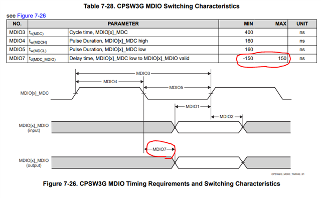
Q2)
Datasheet Table 7-33 to 7-37 provide RGMII timings, but it seems below parameters are not shown.
#1 TskewT: Data to Clock output Skew(at transmitter)
#2 TskewR: Data to Clock input Skew(at Receiver)
#3 Duty Cycle(for 1000BASE)
#4 Rise Time(20-80%)
#5 Fall Time(80-20%)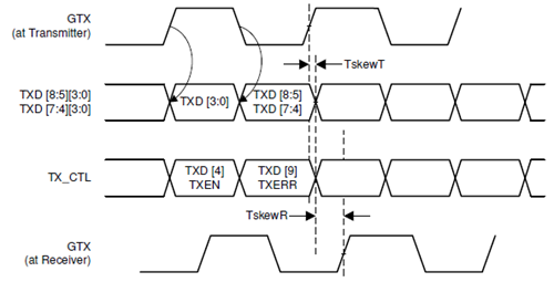
Can you provide these parameters (min/typ/max)?
Thanks and regards,
Koichiro Tashiro


