

Hi,
My customer wants to know Pad diameter of BGA package (ALW).
Please see below diagram.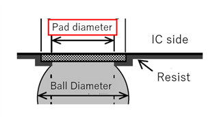
Could you provide this information?
Thanks and regards,
Koichiro Tashiro

- Ask a related questionWhat is a related question?A related question is a question created from another question. When the related question is created, it will be automatically linked to the original question.

