[FAQ] AM625 / AM623 / AM620-Q1 / AM625-Q1 / AM625SIP : Custom board hardware design – Processor power-sequencing requirements for power-up and power-down

Other Parts Discussed in Thread: TPS65220, AM6442, SK-AM62B-P1, AM625, AM625-Q1
  1. Hi TI Experts,

    I have the below queries regarding SOC(Processor) power-sequencing requirements for power-up and power-down

    1.Is there a recommended power sequence to be followed for power-up?
    2.Is there a power supply ramp requirement to be followed for power-up?
    3.Is there a timing requirement to be followed between supply ramps (supply ramp delay time after the previous supply ramps)
    4.Are there any other sequencing requirements that are required to be considered?
    5.Is there a recommended power sequence to be followed for power-down?
    6.Is there a power supply ramp requirement to be followed for power-down?
    7.In the power-down sequence, the MCU_PORz goes low after the power supplies start to ramp down. Is this expected?
    8.Could you comment on the effect of not following the power-up and power-down on SOC (Processor) performance?
    9.Are these recommendations applicable for all the Sitara family of devices

    Let me know your thoughts.

  • Hi Board designers,
    Refer below inputs for the SOC(Processor) power-sequencing requirements for power-up and power-down


    1.Is there a recommended power sequence to be followed for power-up?
    Follow the Power-Up Sequencing Figure and Power-Up Sequencing – Supply / Signal Assignments table of the processor specific data sheet


    2.Is there a power supply ramp requirement to be followed for power-up?
    Refer to Power Supply Slew Rate Requirement section and Power Supply Slew and Slew Rate figure of the processor specific data sheet


    3.Is there a timing requirement to be followed between supply ramps ( supply ramp delay after the previous supply ramps)
    There is not specific timing requirement to be followed between 2 supply ramps. It is recommended to ensure the previous supply ramps and is stable before start of the next supply ramp


    4.Are there any other sequencing requirements that are required to be considered?
    Refer to the notes below the Power-Up Sequencing – Supply / Signal Assignments table of the processor specific data sheet


    5.Is there a recommended power sequence to be followed for power-down?
    Follow the Power-Down Sequencing figure and Power-Down Sequencing – Supply / Signal Assignments table of the processor specific data sheet


    6.Is there a power supply ramp down requirement to be followed for power-down?
    We do not have any specific power supply ramp down requirements to be followed. This is use case dependent.
    The power supply is recommended to be turned on after the supply voltages ramp down below 0.3V.

    The important consideration is following the sequence and Power Supply Slew Rate Requirement.
    The supply rails connect to different internal IP blocks that are powered as the supply ramps.
    Although there is no specified time, it would be recommended to have time that allows the power supply to become stable and also allow time for the internal circuit to setup and complete the configuration.


    7.In the power-down sequence, the MCU_PORz goes low after the power supplies start to ramp down. Is this expected?
    It is drawn that way to represent how things actually work. Power supply supervisors will need to trigger at a voltage that is few percent lower than
    the minimum valid level before it generates a reset. So the reset will occur delayed relative the beginning of the supply falling.
    We expect customers to assert MCU_PORz as soon as possible to ensure the IO cells do not do something unexpected as the IO supply decays.
    So they should pick a threshold for the voltage supervisor that is close to the minimum valid level without being so close that is generates
    false resets. We expect customers to generate reset based on the state of all supplies, where the first one that ramps down will assert reset
    as soon as possible to ensure the device is in a know state as all of the supplies continue to ramp down.


    8.Could you comment on the effect of not following the power-up and power-down on SOC (Processor) performance?
    The data sheet provides the recommend & tested power sequencing diagram that should be followed. We do not characterize the power-up and power-down
    sequence violation as part of the validation. Violating the power down sequence could likely result in issues related to device reliability.
    TI does not collect reliability data on unsupported conditions (i.e. power sequences other than recommended), therefore TI cannot say whether
    the SoC will operate reliably or that it may fail at any time.


    9.Are these recommendations applicable for all the Sitara family of devices
    This is applicable for AM64x, AM62x, AM62Ax, AM62Px

    Regards,

    Sreenivasa

  • Hi Board designers,

    Additional inputs on the supply slew rate:

    The power supply slew rate is only defined for power-up. This slew rate limit is required to prevent the ESD circuits implemented on the power pins from accidently triggering. This is not a concern for power-down.

    Regards,

    Sreenivasa

  • Hi Board designers,

    The power down sequence is being updated to allow the IO supply to ramp down along with the VDD_CORE supply.

    Refer the power-Down sequence in the updated processor specific data sheet.

    Regards,

    Sreenivasa

  • Hi Board designers,

    Input related to decay of power rails

    in our customer project we have the following power-down sequence. All details are shown in the attachment. As the sequence is not properly defined in the datasheet, I have some questions to our sequence:

    * Is the sequence in line with the specification?

    * To which level do we have to discharge the voltages until a next power-up cycle is allowed?

    * What can happen with the SoC, if we don't follow the proper power-down sequence?

    The power-down sequence diagram will be updated in the next revision of the datasheet. The update has already been applied to the AM62Ax and AM62Px datasheets released on ti.com, so you can reference one of these updated power-down diagrams until the AM62x datasheet is updated later this year. We are basically allowing the IO supply to delay their turn-off until the last core supply is turned off. The previous power-down diagram showed the IO supplies being turned off by the time VDD_CORE was turned off. This is still the preferred sequence, if possible, to help prevent the IOs from doing unpredictable things during power-down since logic in the core domain controls the IO functions. However, we found this was difficult to implement and decided the internal circuits that force the IOs to a known state until VDD_CORE ramps-up should perform a similar task during power down when VDD_CORE is lost before the IO supply. We do not want customers leaving IO supplies powered for long periods of time after the VDD_CORE is turned off, so we decided to extend each IO supply turn off until the last core rail is turned off as way to limit the time IO are turned on after VDD_CORE is turned off.    

    It appears you are showing an uncontrolled power-down sequence where all supplies are turned off at the same time, which is consistent with the new power-down diagram as long as you ensure the potential applied to VDDR_CORE is never greater than the potential applied to VDD_CORE + 0.18V during power-up or power-down. This is the only absolute voltage difference that must be managed during power-down.

    The following note will also be added to the next revision of the AM62x datasheet. This note has already been added to the AM62Ax and AM62Px datasheets.

    All power rails must be turned off and decay below 300mV before initiating a new power-up sequence anytime a power rail drops below the minimum value defined in Recommended Operating Conditions. The only exception is when entering/exiting Partial IO low power mode with VDDSHV_CANUART and VDD_CANUART sourced from an always on power source. For this use case the VDDSHV_CANUART and VDD_CANUART power rails are allowed to remain on.

    One issue is, that we can't guarantee the decay down to 300mV. As U18S takes up to 4 sec for decay, there is a high probability to start a new power-up cycle before it reaches 300mV. Can you assess, what can happen in this case? Do you expect any malfunction or damage due to this improper power cycle?

    Our proper power-down cycle, which is implemented in PMIC shuts off all rails at the same time except VDD_CORE. The shut-down of VDD_CORE is delayed by 2ms to guarantee the "old" sequence. Can this be kept?

    I'm not aware of any way this can damage the AM62x device. There could be use cases where this causes a functional issue in your system.

    I also do not anticipate an issue with the AM62x device because the power-on reset input should reset every circuit in the device to the same known state every time reset is asserted. Therefore, the AM62x device should not retain any previous state held by the power not fully decaying. However, this operating condition was not expected and not validated.

    You could encounter system level issues, where other components in your system will not function if you do not allow all supplies to decay. For example: Not allowing the supplies to decay may be a problem for an SD Card connected to AM62x since the SD Card is only reset when you cycle its power, and its supply voltage drops below a specific value defined in the SDIO standard. This is required because SD Cards do not have a reset pin, so they have an internal reset circuit that generates a reset by monitoring the SD Card supply voltage. This can be a problem if the SD Card was previously told to switch to 1.8V IO signaling and you short cycle the power supply such that the AM62x MMCSD host is reset and begins communicating with the SD Card using its default 3.3V IO signaling when the SD Card is still configured to 1.8V signaling because it was not reset.

    We recommend customers design their system to decay below 300mv to minimize any risk of these type of problems.

    Refer below FAQ 

    https://e2e.ti.com/support/processors-group/processors/f/processors-forum/1485094/faq-am62a7-power-rails-decay-note-in-latest-datasheet

    Regards,

    Sreenivasa

  • Hi Board designers,

    Additional inputs:

    (+) AM6442: Power Down Sequence Restrictions - Processors forum - Processors - TI E2E support forums

    The 10ms between VDD_CORE and the 3.3V IO configured in the TPS6522053 PMIC power-down sequence was tested and validated on bench using the AM64 starter kit. For any new or custom PMIC NVM configuration we recommend following the SoC requirement "VDDSHV power rails to turn off as late as the last core supply" because we have not validated a scenario where 3.3V IO stays ON for an extended time (beyond 10ms). 

    The reason why TPS6522053 was configured to turn-off 3.3V IO last is because we wanted to make this PMIC configuration generic for 3.3V and 5V input supply. For example, if customers use a 5V input supply, they can replace the external power-switch with a 3.3V Buck and use the output of this Buck to supply the PMIC LDOs. Turning-OFF the 3.3V last allow customers to use this rail to supply PMIC LDOs, helping to reduce power consumption on applications using 5V input supply.  

    thank you for the clarification. My use case is VSYS=5V so I understand the reason for the deviation. So I think I need to take care that the 3.3V buck discharges the 3.3V rail fast enough in order to minimize the time with 3.3V still present during power off.

    Yes, it is recommended to use a DC/DC with internal active discharge. For example: TPS62A0x.  

    Regards,

    Sreenivasa

  • Sreenvivasa: Should this FAQ also has AM6442 in the title?

    regards

    Jim

  • Hello Jim, 

    I added the below as a note.

    9.Are these recommendations applicable for all the Sitara family of devices
    This is applicable for AM64x, AM62x, AM62Ax, AM62Px

    Let me review and update.

    Regards,

    Sreenivasa

  • Hi Board Designers,

    Inputs related to delay between supply rails for processor power-up sequence

    Input 1

    The VDDS_DDR and VDDS_DDR_C power rails are expected to be powered from the same power source. This waveform shows a grey transition region that begins with the first rising edge and ends with the second rising edge. The supply that powers VDDS_DDR and VDDS_DDR_C can change anywhere in the grey transition region. So it is okay for the the 0.85V supply to ramp before the 1.2V supply.

    Note: We insert multiple transitions within the grey transition region of some waveforms when they represent a transition region for power rails which may receive power from multiple sources. Multiple transitions within the region is used to indicate these power rails can ramp anywhere within the transition region and they do not have any dependency on the other power rails associated with the waveform. Transition regions like the one used for VDDS_DDR and VDDS_DDR_C, indicate all power rails associated with the waveform are powered from a common source and are expected to ramp at the same time anywhere within the transition region.

     The shaded region of the waveform represents a range of time where a supply may ramp up/down relative to other supply rails.  The hatch marks within a shaded region is used to represent multiple power rails just in case all power rails represented by a waveform are not powered from the same source. For example, there may be a reason to power some 1.8V power rails form one source while other 1.8V rails are powered from another source.

    I will be adding legends to this section of the datasheet to describe these two types of transition regions.

    Input 2 

    There is only one firm requirement for AM64x power-down. See note 5 associated with the power-down sequence. 

    The potential applied to VDDR_CORE must never be greater than the potential applied to VDD_CORE + 0.18V during power-up or power-down. This requires VDD_CORE to ramp up before and ramp down after VDDR_CORE when VDD_CORE is operating at 0.75V. VDD_CORE does not have any ramp requirements beyond the one defined for VDDR_CORE. VDD_CORE and VDDR_CORE are expected to be powered by the same source so they ramp together when VDD_CORE is operating at 0.85V.

    Input 3

    Can we share the requirements of timing between the different voltage supply waveforms rising on power-up and falling on power-down. For example, how long after Waveform A rises must Waveform B wait before rising?

    There are no specific timing requirements for these sequencies. The sequence defined in the datasheet is only required to prevent voltage potential differences.

    in Figure  Power-Up Sequencing of the Datasheet, is there  requirements for the time interval of each voltage?
    * Spacing of vertically drawn dashed lines

    No.  No specific time is required between the groups as long as one has ramped before the next begins.

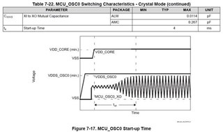
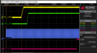
    Customer follow SK-AM62B-P1 design and use same PMIC and found MCU_OSC0 clock start up timing is not matching the sequence we describe in Data Sheet. 

    This is confirmed on both customer board and TI EVM. 

    MCU_OSC0 is supposed to be clocking after VDD_Core rising but the waveform measurement shows it is ahead VDD_CORE.

    Customer would like to get the explanation from TI for this.

    Could team check this or we need to revise data sheet? 

    The datasheet shows it not starting until after the core voltage because there are some cases where the oscillator may not start until VDD_CORE is valid. In most cases it will start as early as VDDS_OSC0, but this may not always be the case.

    This diagram in the datasheet is showing the maximum start-up time, which must include the case where the delay is based on VDD_CORE being valid.

    (+) [FAQ] AM625: Long Term Effects of Simultaneously Power-Down Sequencing of all Voltage Rails - Processors forum - Processors - TI E2E support forums

    AM625: AM6254 power up sequence question

    Will the external circuit(e.g SPI slave side) influence the AM6254 power up sequence? i mean if the SPI or other communication interface(slave side) power up first, will it introduce some current into the AM62 and mess up the AM62 power up sequence? 

    Many of the AM62x pins are not fail-safe and they should not have any potential applied until their respective power rail has ramped to a valid level. For more information refer to the Absolute Maximum Ratings and Recommended Operating Conditions tables in the datasheet.

    (+) AM6442: Powering AM6442BSFFHAALV with TPS6522430RAHRQ1 - Processors forum - Processors - TI E2E support forums

    AM6442: Powering AM6442BSFFHAALV with TPS6522430RAHRQ1

    The processor sequencing requirements can be found in the datasheet under "Power Supply Sequencing". 

    Power Supply Sequencing I can only find the order of the rails.
    However, the delays between the different power supplies are not specified in the datasheet.
    The only delay mentioned is the one between “all supplies valid” and the MCU_PORs (9.5ms).

    Does this mean that the delays between the power supplies themselves don’t matter, and only the sequence is relevant?

    We do not specify the delay between rails. Instead, we have slew rate requirements and sequence order. A supply group must fully ramp to the targeted output voltage with the required slew rate before the next one in sequence start ramping up.   

    AM625-Q1: Power-down sequence

    To which level do we have to discharge the voltages until a next power-up cycle is allowed?

    What can happen with the SoC, if we don't follow the proper power-down sequence?

    The power-down sequence diagram will be updated in the next revision of the datasheet. The update has already been applied to the AM62Ax and AM62Px datasheets released on ti.com, so you can reference one of these updated power-down diagrams until the AM62x datasheet is updated later this year. We are basically allowing the IO supply to delay their turn-off until the last core supply is turned off. The previous power-down diagram showed the IO supplies being turned off by the time VDD_CORE was turned off. This is still the preferred sequence, if possible, to help prevent the IOs from doing unpredictable things during power-down since logic in the core domain controls the IO functions. However, we found this was difficult to implement and decided the internal circuits that force the IOs to a known state until VDD_CORE ramps-up should perform a similar task during power down when VDD_CORE is lost before the IO supply. We do not want customers leaving IO supplies powered for long periods of time after the VDD_CORE is turned off, so we decided to extend each IO supply turn off until the last core rail is turned off as way to limit the time IO are turned on after VDD_CORE is turned off.    

    It appears you are showing an uncontrolled power-down sequence where all supplies are turned off at the same time, which is consistent with the new power-down diagram as long as you ensure the potential applied to VDDR_CORE is never greater than the potential applied to VDD_CORE + 0.18V during power-up or power-down. This is the only absolute voltage difference that must be managed during power-down.

    The following note will also be added to the next revision of the AM62x datasheet. This note has already been added to the AM62Ax and AM62Px datasheets.

    All power rails must be turned off and decay below 300mV before initiating a new power-up sequence anytime a power rail drops below the minimum value defined in Recommended Operating Conditions. The only exception is when entering/exiting Partial IO low power mode with VDDSHV_CANUART and VDD_CANUART sourced from an always on power source. For this use case the VDDSHV_CANUART and VDD_CANUART power rails are allowed to remain on.

    One issue is, that we can't guarantee the decay down to 300mV. As U18S takes up to 4 sec for decay, there is a high probability to start a new power-up cycle before it reaches 300mV. Can you assess, what can happen in this case? Do you expect any malfunction or damage due to this improper power cycle?

    I'm not aware of any way this can damage the AM62x device. There could be use cases where this causes a functional issue in your system.

    I also do not anticipate an issue with the AM62x device because the power-on reset input should reset every circuit in the device to the same known state every time reset is asserted. Therefore, the AM62x device should not retain any previous state held by the power not fully decaying. However, this operating condition was not expected and not validated.

    You could encounter system level issues, where other components in your system will not function if you do not allow all supplies to decay. For example: Not allowing the supplies to decay may be a problem for an SD Card connected to AM62x since the SD Card is only reset when you cycle its power, and its supply voltage drops below a specific value defined in the SDIO standard. This is required because SD Cards do not have a reset pin, so they have an internal reset circuit that generates a reset by monitoring the SD Card supply voltage. This can be a problem if the SD Card was previously told to switch to 1.8V IO signaling and you short cycle the power supply such that the AM62x MMCSD host is reset and begins communicating with the SD Card using its default 3.3V IO signaling when the SD Card is still configured to 1.8V signaling because it was not reset.

    We recommend customers design their system to decay below 300mv to minimize any risk of these type of problems.

    Regards,

    Sreenivasa