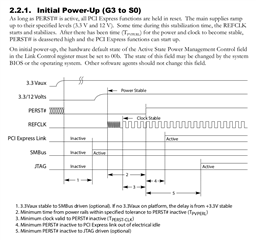
Other Parts Discussed in Thread: TDA4VM,
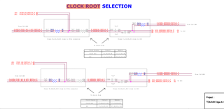
In the TDA4VM SK board, the SOC and the PCIe device connector are connected to a common clock from clock generator (U64).
But the startup code in the BSP downloaded from QNX Software center is configuring the PCIe module to generate the reference clock to PCIe device. Even though the HW and SW configurations are not matching, the PCIe device is getting detected randomly few times (approx 1 in 20 times).
Ref code: \ti-j721e-tda4vm-sk\src\hardware\startup\boards\j721e\sk\hw_init.c
/* REFCLK_DIG_SEL = pma_cmn_refclk_int */
out32(serdes_base_address + CSL_SERDES_RST, in32(serdes_base_address + CSL_SERDES_RST) | CSL_SERDES_RST_REFCLK_DIG_SEL);
/* PLL0_REFCLK_SEL: Selects pma_cmn_refclk_int as reference clock source */
out32(serdes_base_address + CSL_SERDES_RST, in32(serdes_base_address + CSL_SERDES_RST) | CSL_SERDES_RST_PLL0_REFCLK_SEL);
/* PLL1_REFCLK_SEL: Selects pma_cmn_refclk1_int as reference clock source. */
out32(serdes_base_address + CSL_SERDES_RST, in32(serdes_base_address + CSL_SERDES_RST) | CSL_SERDES_RST_PLL1_REFCLK_SEL);
pcie_refclk_to_io(CTRL_MMR0_CFG0_BASE, serdes_id, serdes_id);
/*
* TI J721E-SK
*/
#include "startup.h"
#include "ti_sci.h"
#include "drivers_usbwrapper.h"
#include "J721E_pinmux.h"
#include <hw/omap_i2c.h>
#include "board.h"
#define J721E_WKUP_CTRLMMR_PADCONFIG (0x43000000 + 0x1C000)
#define WKUP_GPIO0_BASE 0x42110000
#define WKUP_GPIO1_BASE 0x42100000
static void init_i2c(void)
{
// pinmux for I2C0
out32(J721E_CTRLMMR_PADCONFIG + PIN_I2C0_SCL, PIN_INPUT_ENABLE | PIN_MODE(0));
out32(J721E_CTRLMMR_PADCONFIG + PIN_I2C0_SDA, PIN_INPUT_ENABLE | PIN_MODE(0));
// pinmux for I2C1
out32(J721E_CTRLMMR_PADCONFIG + PIN_I2C1_SCL, PIN_INPUT_ENABLE | PIN_MODE(0));
out32(J721E_CTRLMMR_PADCONFIG + PIN_I2C1_SDA, PIN_INPUT_ENABLE | PIN_MODE(0));
// pinmux for I2C3
out32(J721E_CTRLMMR_PADCONFIG + PIN_MMC2_CLK, PIN_INPUT_ENABLE | PIN_MODE(4)); // I2C3 SCL
out32(J721E_CTRLMMR_PADCONFIG + PIN_MMC2_CMD, PIN_INPUT_ENABLE | PIN_MODE(4)); // I2C3 SDA
// pinmux for I2C5
out32(J721E_CTRLMMR_PADCONFIG + PIN_PRG0_MDIO0_MDIO, PIN_INPUT_ENABLE | PIN_MODE(2)); // I2C5 SCL pin Y26
out32(J721E_CTRLMMR_PADCONFIG + PIN_PRG0_MDIO0_MDC, PIN_INPUT_ENABLE | PIN_MODE(2)); // I2C5 SDA pin AA27
}
static void init_gpu(void)
{
if (ti_sci_set_device_state(TISCI_DEV_GPU0_GPU_0, 0, MSG_DEVICE_SW_STATE_ON) == -1) {
kprintf("%s: Set GPU0 device state failed!\n", __func__);
}
if (ti_sci_set_device_state(TISCI_DEV_GPU0_GPUCORE_0, 0, MSG_DEVICE_SW_STATE_ON) == -1) {
kprintf("%s: Set GPU1 device state failed!\n", __func__);
}
}
static const uint8_t hdmi_pins[] = {
PIN_PRG1_PRU0_GPO8, // offset 0x24: VOUT0_DATA22
PIN_PRG1_PRU0_GPO9, // offset 0x28: VOUT0_DATA23
PIN_PRG1_PRU0_GPO11, // offset 0x30: VOUT0_DATA16
PIN_PRG1_PRU0_GPO12, // offset 0x34: VOUT0_DATA17
PIN_PRG1_PRU0_GPO13, // offset 0x38: VOUT0_DATA18
PIN_PRG1_PRU0_GPO14, // offset 0x3C: VOUT0_DATA19
PIN_PRG1_PRU0_GPO15, // offset 0x40: VOUT0_DATA20
PIN_PRG1_PRU0_GPO16, // offset 0x44: VOUT0_DATA21
PIN_PRG1_PRU1_GPO0, // offset 0x58: VOUT0_DATA0
PIN_PRG1_PRU1_GPO1, // offset 0x5C: VOUT0_DATA1
PIN_PRG1_PRU1_GPO2, // offset 0x60: VOUT0_DATA3
PIN_PRG1_PRU1_GPO3, // offset 0x64: VOUT0_DATA3
PIN_PRG1_PRU1_GPO4, // offset 0x68: VOUT0_DATA4
PIN_PRG1_PRU1_GPO5, // offset 0x6C: VOUT0_DATA5
PIN_PRG1_PRU1_GPO6, // offset 0x70: VOUT0_DATA6
PIN_PRG1_PRU1_GPO7, // offset 0x74: VOUT0_DATA7
PIN_PRG1_PRU1_GPO8, // offset 0x78: VOUT0_DATA8
PIN_PRG1_PRU1_GPO9, // offset 0x7C: VOUT0_DATA9
PIN_PRG1_PRU1_GPO10, // offset 0x80: VOUT0_DATA10
PIN_PRG1_PRU1_GPO11, // offset 0x84: VOUT0_DATA11
PIN_PRG1_PRU1_GPO12, // offset 0x88: VOUT0_DATA12
PIN_PRG1_PRU1_GPO13, // offset 0x8C: VOUT0_DATA13
PIN_PRG1_PRU1_GPO14, // offset 0x90: VOUT0_DATA14
PIN_PRG1_PRU1_GPO15, // offset 0x94: VOUT0_DATA15
PIN_PRG1_PRU1_GPO16, // offset 0x98: VOUT0_HSYNC
PIN_PRG1_PRU1_GPO17, // offset 0x9C: VOUT0_DE
PIN_PRG1_PRU1_GPO18, // offset 0xA0: VOUT0_VSYNC
PIN_PRG1_PRU1_GPO19 // offset 0xA4: VOUT0_PCLK
};
static int init_dss(void)
{
// DSS power, functional clock
if (ti_sci_set_device_state(TISCI_DEV_DSS0, 0, MSG_DEVICE_SW_STATE_ON) == -1) {
kprintf("%s: Set DSS device state failed!\n", __func__);
return -1;
}
if (ti_sci_set_clock_state(TISCI_DEV_DSS0, TISCI_DEV_DSS0_DSS_FUNC_CLK,
0, MSG_CLOCK_SW_STATE_REQ) == -1) {
kprintf("%s: Set DSS clock state failed!\n", __func__);
return -1;
}
return 0;
}
#define SK_HDMI_HPD_PIN_NUM 0U
#define SK_HDMI_PDN_PIN_NUM 127U
#define SK_HDMI_LS_OE_PIN_NUM 87U
static int init_hdmi(void)
{
const uint32_t hdmi_pincfg = PIN_INPUT_ENABLE | PIN_MODE(10);
uint8_t pin;
// Pinmux
for (pin = 0; pin < sizeof(hdmi_pins) / sizeof(uint8_t); pin++) {
out32(J721E_CTRLMMR_PADCONFIG + hdmi_pins[pin], hdmi_pincfg);
}
/* HDMI_HPD */
out32(J721E_CTRLMMR_PADCONFIG + PIN_UART1_RTSN, PIN_INPUT_ENABLE | PIN_MODE(7));
// GPIO1_0 as input
out32(J721E_GPIO1_BASE + J721E_GPIO_DIR(SK_HDMI_HPD_PIN_NUM),
in32(J721E_GPIO1_BASE + J721E_GPIO_DIR(SK_HDMI_HPD_PIN_NUM)) | J721E_GPIO_BIT(SK_HDMI_HPD_PIN_NUM));
// Default signal voltage 3.3v, output low
out32(J721E_GPIO1_BASE + J721E_GPIO_SET_DATA(SK_HDMI_HPD_PIN_NUM), (J721E_GPIO_BIT(SK_HDMI_HPD_PIN_NUM)));
/* HDMI_PDn */
out32(J721E_CTRLMMR_PADCONFIG + PIN_UART1_CTSN, PIN_INPUT_ENABLE | PIN_MODE(7));
// GPIO0_127 as output
out32(J721E_GPIO0_BASE + J721E_GPIO_DIR(SK_HDMI_PDN_PIN_NUM),
in32(J721E_GPIO0_BASE + J721E_GPIO_DIR(SK_HDMI_PDN_PIN_NUM)) & ~(J721E_GPIO_BIT(SK_HDMI_PDN_PIN_NUM)));
// Default signal voltage 3.3v, output low
out32(J721E_GPIO0_BASE + J721E_GPIO_SET_DATA(SK_HDMI_PDN_PIN_NUM), (J721E_GPIO_BIT(SK_HDMI_PDN_PIN_NUM)));
/* HDMI_LS_OE */
// GPIO0_87 as output
out32(J721E_GPIO0_BASE + J721E_GPIO_DIR(SK_HDMI_LS_OE_PIN_NUM),
in32(J721E_GPIO0_BASE + J721E_GPIO_DIR(SK_HDMI_LS_OE_PIN_NUM)) & ~(J721E_GPIO_BIT(SK_HDMI_LS_OE_PIN_NUM)));
// Default signal voltage 3.3v, output low
out32(J721E_GPIO0_BASE + J721E_GPIO_SET_DATA(SK_HDMI_LS_OE_PIN_NUM), (J721E_GPIO_BIT(SK_HDMI_LS_OE_PIN_NUM)));
if (ti_sci_cmd_set_clk_parent(TISCI_DEV_DSS0, TISCI_DEV_DSS0_DSS_INST0_DPI_1_IN_2X_CLK,
TISCI_DEV_DSS0_DSS_INST0_DPI_1_IN_2X_CLK_PARENT_DPI0_EXT_CLKSEL_OUT0) == -1) {
kprintf("%s: Set DSS clock parent failed!\n", __func__);
return -1;
}
// Set 148.48Mhz pixel clock for 1080P output
if (ti_sci_cmd_clk_set_freq(TISCI_DEV_DSS0, TISCI_DEV_DSS0_DSS_INST0_DPI_1_IN_2X_CLK,
148480000ULL, 148480000ULL, 148480000ULL) == -1) {
kprintf("%s: Set DSS pixel clock frequency failed!\n", __func__);
return -1;
}
if (ti_sci_set_clock_state(TISCI_DEV_DSS0, TISCI_DEV_DSS0_DSS_INST0_DPI_1_IN_2X_CLK,
0, MSG_CLOCK_SW_STATE_REQ) == -1) {
kprintf("%s: Set DSS clock state failed!\n", __func__);
return -1;
}
return 0;
}
static int init_dp(void)
{
// Set HPD pin
out32(J721E_CTRLMMR_PADCONFIG + PIN_SPI0_CS1, PIN_INPUT_ENABLE | PIN_MODE(5));
// Enable DSS EDP0
if (ti_sci_set_device_state(TISCI_DEV_DSS_EDP0, 0, MSG_DEVICE_SW_STATE_ON) == -1) {
kprintf("%s: Set DSS DP device state failed!\n", __func__);
return -1;
}
// Enable SERDES 10G0
if (ti_sci_set_device_state(TISCI_DEV_SERDES_10G0, 0, MSG_DEVICE_SW_STATE_ON) == -1) {
kprintf("%s: Set SERDES device state failed!\n", __func__);
return -1;
}
if (ti_sci_cmd_set_clk_parent(TISCI_DEV_DSS0, TISCI_DEV_DSS0_DSS_INST0_DPI_2_IN_2X_CLK,
TISCI_DEV_DSS0_DSS_INST0_DPI_2_IN_2X_CLK_PARENT_HSDIV1_16FFT_MAIN_18_HSDIVOUT0_CLK) == -1) {
kprintf("%s: Set DSS clock parent failed!\n", __func__);
return -1;
}
if (ti_sci_cmd_set_clk_parent(TISCI_DEV_DSS0, TISCI_DEV_DSS0_DSS_INST0_DPI_3_IN_2X_CLK,
TISCI_DEV_DSS0_DSS_INST0_DPI_3_IN_2X_CLK_PARENT_DPI1_EXT_CLKSEL_OUT0) == -1) {
kprintf("%s: Set DSS clock parent failed!\n", __func__);
return -1;
}
if (ti_sci_cmd_set_clk_parent(TISCI_DEV_DSS0, TISCI_DEV_DSS0_DSS_INST0_DPI_0_IN_2X_CLK,
TISCI_DEV_DSS0_DSS_INST0_DPI_0_IN_2X_CLK_PARENT_HSDIV1_16FFT_MAIN_16_HSDIVOUT0_CLK) == -1) {
kprintf("%s: Set DSS clock parent failed!\n", __func__);
return -1;
}
// Set 119Mhz pixel clock for 1680x1050 output
if (ti_sci_cmd_clk_set_freq(TISCI_DEV_DSS0, TISCI_DEV_DSS0_DSS_INST0_DPI_0_IN_2X_CLK,
119000000ULL, 119000000ULL, 119000000ULL) == -1) {
kprintf("%s: Set DSS pixel clock frequency failed!\n", __func__);
return -1;
}
if (ti_sci_set_clock_state(TISCI_DEV_DSS0, TISCI_DEV_DSS0_DSS_INST0_DPI_0_IN_2X_CLK,
0, MSG_CLOCK_SW_STATE_REQ) == -1) {
kprintf("%s: Set DSS clock state failed!\n", __func__);
return -1;
}
return 0;
}
static const uint8_t ospi_pins[] = {
PIN_MCU_OSPI0_CLK,
// PIN_MCU_OSPI0_LBCLKO,
PIN_MCU_OSPI0_DQS,
PIN_MCU_OSPI0_D0,
PIN_MCU_OSPI0_D1,
PIN_MCU_OSPI0_D2,
PIN_MCU_OSPI0_D3,
PIN_MCU_OSPI0_D4,
PIN_MCU_OSPI0_D5,
PIN_MCU_OSPI0_D6,
PIN_MCU_OSPI0_D7,
PIN_MCU_OSPI0_CSN0
};
static void init_ospi(void)
{
const paddr_t padcfg_base = J721E_WKUP_CTRLMMR_PADCONFIG;
uint8_t pin;
// Set reference clock parent
if (ti_sci_cmd_set_clk_parent(TISCI_DEV_MCU_FSS0_OSPI_0, TISCI_DEV_MCU_FSS0_OSPI_0_OSPI_RCLK_CLK,
TISCI_DEV_MCU_FSS0_OSPI_0_OSPI_RCLK_CLK_PARENT_HSDIV4_16FFT_MCU_2_HSDIVOUT4_CLK) == -1) {
kprintf("%s: Set OSPI0 RCLK clock parent failed!\n", __func__);
return;
}
// Set 200Mhz reference clock
if (ti_sci_cmd_clk_set_freq(TISCI_DEV_MCU_FSS0_OSPI_0, TISCI_DEV_MCU_FSS0_OSPI_0_OSPI_RCLK_CLK,
200000000ULL, 200000000ULL, 200000000ULL) == -1) {
kprintf("%s: Set OSPI0 RCLK frequency failed!\n", __func__);
return;
}
// Pinmux
for (pin = 0; pin < sizeof(ospi_pins) / sizeof(uint8_t); pin++) {
if ((ospi_pins[pin] == PIN_MCU_OSPI0_CLK) || (ospi_pins[pin] == PIN_MCU_OSPI0_CSN0)) {
out32(padcfg_base + ospi_pins[pin], PIN_MODE(0));
} else {
out32(padcfg_base + ospi_pins[pin], PIN_INPUT_ENABLE | PIN_MODE(0));
}
}
}
#define SK_SDIO_1V8_EN_PIN_NUM (9U)
static void init_sdmmc(void)
{
// pinmux for SD(MMC1)
out32(J721E_CTRLMMR_PADCONFIG + PIN_MMC1_CMD, PIN_PULL_DISABLE | PIN_INPUT_ENABLE | PIN_MODE(0));
out32(J721E_CTRLMMR_PADCONFIG + PIN_MMC1_CLK, PIN_PULL_DISABLE | PIN_INPUT_ENABLE | PIN_MODE(0));
out32(J721E_CTRLMMR_PADCONFIG + PIN_MMC1_CLKLB, PIN_PULL_DISABLE | PIN_INPUT_ENABLE | PIN_MODE(0));
out32(J721E_CTRLMMR_PADCONFIG + PIN_MMC1_DAT0, PIN_PULL_DISABLE | PIN_INPUT_ENABLE | PIN_MODE(0));
out32(J721E_CTRLMMR_PADCONFIG + PIN_MMC1_DAT1, PIN_PULL_DISABLE | PIN_INPUT_ENABLE | PIN_MODE(0));
out32(J721E_CTRLMMR_PADCONFIG + PIN_MMC1_DAT2, PIN_PULL_DISABLE | PIN_INPUT_ENABLE | PIN_MODE(0));
out32(J721E_CTRLMMR_PADCONFIG + PIN_MMC1_DAT3, PIN_PULL_DISABLE | PIN_INPUT_ENABLE | PIN_MODE(0));
out32(J721E_CTRLMMR_PADCONFIG + PIN_MMC1_SDCD, PIN_PULL_DISABLE | PIN_INPUT_ENABLE | PIN_MODE(0));
// WKUP_GPIO0_9 for signal voltage switch
out32(J721E_WKUP_CTRLMMR_PADCONFIG + 0xd4, PIN_PULL_DISABLE | PIN_MODE(7));
// WKUP_GPIO0_9 as output
out32(WKUP_GPIO0_BASE + J721E_GPIO_DIR(SK_SDIO_1V8_EN_PIN_NUM),
in32(WKUP_GPIO0_BASE + J721E_GPIO_DIR(SK_SDIO_1V8_EN_PIN_NUM)) & ~(J721E_GPIO_BIT(SK_SDIO_1V8_EN_PIN_NUM)));
// Default signal voltage 3.3v, output high
out32(WKUP_GPIO0_BASE + J721E_GPIO_SET_DATA(SK_SDIO_1V8_EN_PIN_NUM), J721E_GPIO_BIT(SK_SDIO_1V8_EN_PIN_NUM));
}
static void init_trng(void)
{
uint32_t clcnt, resets;
uint8_t p_state, c_state;
// SA2_UL
if (ti_sci_get_device_state(TISCI_DEV_SA2_UL0, &clcnt, &resets, &p_state, &c_state) == -1) {
kprintf("%s: get_device_state failed! %d\n", __func__, __LINE__);
return;
}
if (c_state == MSG_DEVICE_HW_STATE_OFF) {
if (ti_sci_set_device_state(TISCI_DEV_SA2_UL0, MSG_FLAG_DEVICE_RESET_ISO, MSG_DEVICE_SW_STATE_ON) == -1) {
kprintf("%s: set_device_state failed! %d\n", __func__, __LINE__);
return;
}
if (ti_sci_set_device_resets(TISCI_DEV_SA2_UL0, 0) == -1) {
kprintf("%s: set_device_resets failed! %d\n", __func__, __LINE__);
return;
}
}
ti_sci_set_clock_state(TISCI_DEV_SA2_UL0, TISCI_DEV_SA2_UL0_X2_CLK, 0, MSG_CLOCK_SW_STATE_REQ);
ti_sci_set_clock_state(TISCI_DEV_SA2_UL0, TISCI_DEV_SA2_UL0_X1_CLK, 0, MSG_CLOCK_SW_STATE_REQ);
}
static void serdes_cycle_delay (const uint64_t count)
{
volatile uint64_t sat = 0;
for(sat=0;sat<count;sat++);
}
static void serdes_lane_enable (const uintptr_t serdes_base_address)
{
uint32_t lane_num, tmp;
/* Enable lanes in register */
for(lane_num = 0; lane_num < CSL_SERDES_MAX_LANES; lane_num++)
{
if ((SERDES_DIAG_PCIE_LANE_MASK & (1 << lane_num)) !=0)
{
/* PIPE should only enable P0/P1 enable */
tmp = in32(serdes_base_address + CSL_SERDES_LANECTL0 + (0x40 * lane_num));
tmp |= CSL_SERDES_LANECTL0_P0_ENABLE_MASK;
out32(serdes_base_address + CSL_SERDES_LANECTL0 + (0x40 * lane_num), tmp);
}
}
/* Release PHY Reset*/
out32(serdes_base_address + CSL_SERDES_RST, (in32(serdes_base_address + CSL_SERDES_RST) | CSL_SERDES_RST_PHY_RESET_N) );
serdes_cycle_delay(100);
}
static void pcie_refclk_to_io(const uint32_t baseaddress, const uint32_t serdes_instance, const uint32_t ref_clk)
{
uint32_t reg;
switch(serdes_instance) {
case 0:
reg = ref_clk;
/* Enable output clock */
reg |= CSL_MAIN_CTRL_MMR_CFG0_PCIE_REFCLK0_CLKSEL_OUT_CLK_EN;
out32(baseaddress + CSL_MAIN_CTRL_MMR_CFG0_PCIE_REFCLK0_CLKSEL, reg);
out32(baseaddress + CTRLMMR_ACSPCIE0_CTRL, (in32(baseaddress + CTRLMMR_ACSPCIE0_CTRL) & 0xFFFFFFFC));
break;
case 1:
reg = ref_clk;
/* Enable output clock */
reg |= CSL_MAIN_CTRL_MMR_CFG0_PCIE_REFCLK1_CLKSEL_OUT_CLK_EN;
out32(baseaddress + CSL_MAIN_CTRL_MMR_CFG0_PCIE_REFCLK1_CLKSEL, reg);
out32(baseaddress + CTRLMMR_ACSPCIE0_CTRL, (in32(baseaddress + CTRLMMR_ACSPCIE0_CTRL) & 0xFFFFFFFC));
break;
case 2:
reg = ref_clk;
/* Enable output clock */
reg |= CSL_MAIN_CTRL_MMR_CFG0_PCIE_REFCLK2_CLKSEL_OUT_CLK_EN;
out32(baseaddress + CSL_MAIN_CTRL_MMR_CFG0_PCIE_REFCLK2_CLKSEL, reg);
out32(baseaddress + CTRLMMR_ACSPCIE0_CTRL, (in32(baseaddress + CTRLMMR_ACSPCIE0_CTRL) & 0xFFFFFFFC));
break;
case 3:
reg = ref_clk;
/* Enable output clock */
reg |= CSL_MAIN_CTRL_MMR_CFG0_PCIE_REFCLK3_CLKSEL_OUT_CLK_EN;
out32(baseaddress + CSL_MAIN_CTRL_MMR_CFG0_PCIE_REFCLK3_CLKSEL, reg);
out32(baseaddress + CTRLMMR_ACSPCIE0_CTRL, (in32(baseaddress + CTRLMMR_ACSPCIE0_CTRL) & 0xFFFFFFFC));
break;
default:
break;
}
}
#define SK_PCIE_0_M2_RTSZ_PIN_NUM (72U)
#define SK_PCIE_1_M2_RTSZ_PIN_NUM (11U)
static void init_pci(const uint8_t serdes_id)
{
uint32_t tmp;
uint32_t lane_num;
const uintptr_t serdes_base_address = CSL_SERDES_16G0_BASE + (serdes_id * 0x10000UL);
if (serdes_id > 2) {
kprintf("%s: serdes_%d is invalid!\n", __func__, serdes_id);
return;
}
/* Configure SERDES*/
switch(serdes_id) {
case 0:
if (ti_sci_set_device_state(TISCI_DEV_SERDES_16G0, 0, MSG_DEVICE_SW_STATE_ON) == -1) {
kprintf("%s: Set SERDES_16G0 device state failed!\n", __func__);
return;
}
if (ti_sci_cmd_set_clk_parent(TISCI_DEV_SERDES_16G0, TISCI_DEV_SERDES_16G0_CORE_REF_CLK,
TISCI_DEV_SERDES_16G0_CORE_REF_CLK_PARENT_HSDIV4_16FFT_MAIN_2_HSDIVOUT4_CLK) == -1) {
kprintf("%s: Set SERDES_16G0 ref clock parent failed!\n", __func__);
return;
}
if (ti_sci_set_clock_state(TISCI_DEV_SERDES_16G0, TISCI_DEV_SERDES_16G0_CORE_REF_CLK,
0, MSG_CLOCK_SW_STATE_AUTO) == -1) {
kprintf("%s: Set SERDES_16G0 ref clock state failed!\n", __func__);
return;
}
if (ti_sci_cmd_set_clk_parent(TISCI_DEV_SERDES_16G0, TISCI_DEV_SERDES_16G0_CORE_REF1_CLK,
TISCI_DEV_SERDES_16G0_CORE_REF1_CLK_PARENT_HSDIV4_16FFT_MAIN_2_HSDIVOUT4_CLK) == -1) {
kprintf("%s: Set SERDES_16G0 ref1 clock parent failed!\n", __func__);
return;
}
if (ti_sci_set_clock_state(TISCI_DEV_SERDES_16G0, TISCI_DEV_SERDES_16G0_CORE_REF1_CLK,
0, MSG_CLOCK_SW_STATE_AUTO) == -1) {
kprintf("%s: Set SERDES_16G0 ref1 clock state failed!\n", __func__);
return;
}
kprintf("\n SK PCIe0 GPIO enabling \n");
// Setting PAD Config GPIO0_72 for SOC_PCIe0_M.2_RTSz
out32(J721E_CTRLMMR_PADCONFIG + PIN_PRG0_PRU1_GPO9, PIN_PULL_DIRECTION | PIN_PULL_DISABLE | PIN_MODE(7));
//Setting GPIO0_72 as output
out32(J721E_GPIO0_BASE + J721E_GPIO_DIR(SK_PCIE_0_M2_RTSZ_PIN_NUM),
in32(J721E_GPIO0_BASE + J721E_GPIO_DIR(SK_PCIE_0_M2_RTSZ_PIN_NUM)) & ~(J721E_GPIO_BIT(SK_PCIE_0_M2_RTSZ_PIN_NUM)));
// Default signal voltage 3.3v, output high
out32(J721E_GPIO0_BASE + J721E_GPIO_SET_DATA(SK_PCIE_0_M2_RTSZ_PIN_NUM), J721E_GPIO_BIT(SK_PCIE_0_M2_RTSZ_PIN_NUM));
break;
case 1:
if (ti_sci_set_device_state(TISCI_DEV_SERDES_16G1, 0, MSG_DEVICE_SW_STATE_ON) == -1) {
kprintf("%s: Set SERDES_16G1 device state failed!\n", __func__);
return;
}
if (ti_sci_cmd_set_clk_parent(TISCI_DEV_SERDES_16G1, TISCI_DEV_SERDES_16G1_CORE_REF_CLK,
TISCI_DEV_SERDES_16G1_CORE_REF_CLK_PARENT_HSDIV4_16FFT_MAIN_2_HSDIVOUT4_CLK) == -1) {
kprintf("%s: Set SERDES_16G1 ref clock parent failed!\n", __func__);
return;
}
if (ti_sci_set_clock_state(TISCI_DEV_SERDES_16G1, TISCI_DEV_SERDES_16G1_CORE_REF_CLK,
0, MSG_CLOCK_SW_STATE_AUTO) == -1) {
kprintf("%s: Set SERDES_16G1 ref clock state failed!\n", __func__);
return;
}
if (ti_sci_cmd_set_clk_parent(TISCI_DEV_SERDES_16G1, TISCI_DEV_SERDES_16G1_CORE_REF1_CLK,
TISCI_DEV_SERDES_16G1_CORE_REF1_CLK_PARENT_HSDIV4_16FFT_MAIN_2_HSDIVOUT4_CLK) == -1) {
kprintf("%s: Set SERDES_16G1 ref1 clock parent failed!\n", __func__);
return;
}
if (ti_sci_set_clock_state(TISCI_DEV_SERDES_16G1, TISCI_DEV_SERDES_16G1_CORE_REF1_CLK,
0, MSG_CLOCK_SW_STATE_AUTO) == -1) {
kprintf("%s: Set SERDES_16G1 ref1 clock state failed!\n", __func__);
return;
}
// Setting PAD CONFIG WKUP_GPIO0_11 for SOC_PCIe1_M.2_RTSz
out32(J721E_WKUP_CTRLMMR_PADCONFIG + PIN_WKUP_GPIO0_11, PIN_PULL_DIRECTION | PIN_PULL_DISABLE | PIN_MODE(7));
// Setting WKUP_GPIO0_11 as Output
out32(WKUP_GPIO0_BASE + J721E_GPIO_DIR(SK_PCIE_1_M2_RTSZ_PIN_NUM),
in32(WKUP_GPIO0_BASE + J721E_GPIO_DIR(SK_PCIE_1_M2_RTSZ_PIN_NUM)) & ~(J721E_GPIO_BIT(SK_PCIE_1_M2_RTSZ_PIN_NUM)));
// Default signal voltage 3.3v, output high
out32(WKUP_GPIO0_BASE + J721E_GPIO_SET_DATA(SK_PCIE_1_M2_RTSZ_PIN_NUM), J721E_GPIO_BIT(SK_PCIE_1_M2_RTSZ_PIN_NUM));
break;
case 2:
if (ti_sci_set_device_state(TISCI_DEV_SERDES_16G2, 0, MSG_DEVICE_SW_STATE_ON) == -1) {
kprintf("%s: Set SERDES_16G2 device state failed!\n", __func__);
return;
}
if (ti_sci_cmd_set_clk_parent(TISCI_DEV_SERDES_16G2, TISCI_DEV_SERDES_16G2_CORE_REF_CLK,
TISCI_DEV_SERDES_16G2_CORE_REF_CLK_PARENT_HSDIV4_16FFT_MAIN_2_HSDIVOUT4_CLK) == -1) {
kprintf("%s: Set SERDES_16G2 ref clock parent failed!\n", __func__);
return;
}
if (ti_sci_set_clock_state(TISCI_DEV_SERDES_16G2, TISCI_DEV_SERDES_16G2_CORE_REF_CLK,
0, MSG_CLOCK_SW_STATE_AUTO) == -1) {
kprintf("%s: Set SERDES_16G2 ref clock state failed!\n", __func__);
return;
}
if (ti_sci_cmd_set_clk_parent(TISCI_DEV_SERDES_16G2, TISCI_DEV_SERDES_16G2_CORE_REF1_CLK,
TISCI_DEV_SERDES_16G2_CORE_REF1_CLK_PARENT_HSDIV4_16FFT_MAIN_2_HSDIVOUT4_CLK) == -1) {
kprintf("%s: Set SERDES_16G2 ref1 clock parent failed!\n", __func__);
return;
}
if (ti_sci_set_clock_state(TISCI_DEV_SERDES_16G2, TISCI_DEV_SERDES_16G2_CORE_REF1_CLK,
0, MSG_CLOCK_SW_STATE_AUTO) == -1) {
kprintf("%s: Set SERDES_16G2 ref1 clock state failed!\n", __func__);
return;
}
break;
default:
kprintf("%s: serdes_%d is invalid!\n", __func__, serdes_id);
return;
}
/* CSL_serdesPorReset */
out32(serdes_base_address + CSL_SERDES_CTRL, in32(serdes_base_address + CSL_SERDES_CTRL) | CSL_SERDES_CTRL_POR_EN);
serdes_cycle_delay(1000);
out32(serdes_base_address + CSL_SERDES_CTRL, in32(serdes_base_address + CSL_SERDES_CTRL) & ~(CSL_SERDES_CTRL_POR_EN));
/* CSL_serdesRefclkSel */
/* refClk == CSL_SERDES_REF_CLOCK_100M - 100MHz clock */
tmp = in32(serdes_base_address + CSL_SERDES_TOP_CTRL);
tmp &= ~(CSL_SERDES_TOP_CTRL_PMA_CMN_REFCLK_DIG_DIV_MASK);
out32(serdes_base_address + CSL_SERDES_TOP_CTRL, (tmp | (0x2 << CSL_SERDES_TOP_CTRL_PMA_CMN_REFCLK_DIG_DIV_SHIFT)));
/* PMA_CMN_REFCLK_INT_MODE */
/* 100MHz and greater reference clock */
tmp = in32(serdes_base_address + CSL_SERDES_TOP_CTRL);
tmp &= ~(CSL_SERDES_TOP_CTRL_PMA_CMN_REFCLK_INT_MODE_MASK);
out32(serdes_base_address + CSL_SERDES_TOP_CTRL, (tmp | (0x1 << CSL_SERDES_TOP_CTRL_PMA_CMN_REFCLK_INT_MODE_SHIFT)));
/* REFCLK_DIG_SEL = pma_cmn_refclk_int */
out32(serdes_base_address + CSL_SERDES_RST, in32(serdes_base_address + CSL_SERDES_RST) | CSL_SERDES_RST_REFCLK_DIG_SEL);
/* PLL0_REFCLK_SEL: Selects pma_cmn_refclk_int as reference clock source */
out32(serdes_base_address + CSL_SERDES_RST, in32(serdes_base_address + CSL_SERDES_RST) | CSL_SERDES_RST_PLL0_REFCLK_SEL);
/* PLL1_REFCLK_SEL: Selects pma_cmn_refclk1_int as reference clock source. */
out32(serdes_base_address + CSL_SERDES_RST, in32(serdes_base_address + CSL_SERDES_RST) | CSL_SERDES_RST_PLL1_REFCLK_SEL);
/* Wait 1us before writing to CMN registers */
serdes_cycle_delay(1000);
/* Assert PHY reset and disable all lanes */
out32(serdes_base_address + CSL_SERDES_RST, in32(serdes_base_address + CSL_SERDES_RST) & ~(CSL_SERDES_RST_PHY_RESET_N));
for(lane_num = 0; lane_num < SERDES_DIAG_PCIE_NUM_LANES; lane_num++)
{
if ((SERDES_DIAG_PCIE_LANE_MASK & (1 << lane_num))!=0)
{
tmp = in32(serdes_base_address + CSL_SERDES_LANECTL0 + (0x40 * lane_num));
tmp &= ~(CSL_SERDES_LANECTL0_P0_FORCE_ENABLE_MASK | CSL_SERDES_LANECTL0_P0_ENABLE_MASK);
out32(serdes_base_address + CSL_SERDES_LANECTL0 + (0x40 * lane_num), tmp);
}
}
/*Load the Serdes Config File */
tmp = in32(serdes_base_address + CSL_SERDES_CMN_PLLLC_LF_COEFF_MODE1_PREG__CMN_PLLLC_MODE_PREG);
tmp &= 0xFFFF;
tmp |= (0x5U << CSL_SERDES_CMN_PLLLC_LF_CMN_PLLLC_LF_INTCOEFF_MODE1_PREG_SHIFT);
tmp |= (0x10U << CSL_SERDES_CMN_PLLLC_LF_CMN_PLLLC_LF_PROPFRAC_MODE1_PREG_SHIFT);
tmp |= (0x2U << CSL_SERDES_CMN_PLLLC_LF_CMN_PLLLC_LF_CMN_PLLLC_LF_PROPCOEFF_MODE1_PREG);
out32(serdes_base_address + CSL_SERDES_CMN_PLLLC_LF_COEFF_MODE1_PREG__CMN_PLLLC_MODE_PREG, tmp);
tmp = in32(serdes_base_address + CSL_SERDES_CMN_PLLLC_LOCK_CNTSTART_PREG__CMN_PLLLC_LF_COEFF_MODE0_PREG);
tmp &= 0xFFFF0000;
tmp |= (0x5U << CSL_SERDES_CMN_PLLLC_LOCK_CMN_PLLLC_LF_INTCOEFF_MODE0_PREG);
tmp |= (0x10U << CSL_SERDES_CMN_PLLLC_LOCK_CMN_PLLLC_LF_PROPFRAC_MODE0_PREG);
tmp |= (0x2U << CSL_SERDES_CMN_PLLLC_LOCK_CMN_PLLLC_LF_PROPCOEFF_MODE0_PREG);
out32(serdes_base_address + CSL_SERDES_CMN_PLLLC_LOCK_CNTSTART_PREG__CMN_PLLLC_LF_COEFF_MODE0_PREG, tmp);
tmp = in32(serdes_base_address + CSL_SERDES_CMN_PLLLC_BWCAL_MODE1_PREG__CMN_PLLLC_CLK0_PREG);
tmp &= 0xFFFF;
tmp |= (0x6U << CSL_SERDES_CMN_PLLLC_BWCAL_MODE1_CMN_PLLLC_BWCAL_TMR_MODE1_PREG_SHIFT);
tmp |= (0xAU << CSL_SERDES_CMN_PLLLC_BWCAL_MODE1_CMN_PLLLC_BWCAL_THRESH_MODE1_PREG_SHIFT);
tmp |= (0x1U << CSL_SERDES_CMN_PLLLC_BWCAL_MODE1_CMN_PLLLC_BWCAL_EN_MODE1_PREG_SHIFT);
out32(serdes_base_address + CSL_SERDES_CMN_PLLLC_BWCAL_MODE1_PREG__CMN_PLLLC_CLK0_PREG, tmp);
tmp = in32(serdes_base_address + CSL_SERDES_CMN_PLLLC_DSMCORR_PREG__CMN_PLLLC_BWCAL_MODE0_PREG);
tmp &= 0xFFFF0000;
tmp |= (0x6U << CSL_SERDES_CMN_PLLLC_DSMCORR_PREG_CMN_PLLLC_BWCAL_TMR_MODE0_PREG_SHIFT);
tmp |= (0xAU << CSL_SERDES_CMN_PLLLC_DSMCORR_PREG_CMN_PLLLC_BWCAL_THRESH_MODE0_PREG_SHIFT);
tmp |= (0x1U << CSL_SERDES_CMN_PLLLC_DSMCORR_PREG_CMN_PLLLC_BWCAL_EN_MODE0_PREG_SHIFT);
out32(serdes_base_address + CSL_SERDES_CMN_PLLLC_DSMCORR_PREG__CMN_PLLLC_BWCAL_MODE0_PREG, tmp);
/* Set this to standard mode defined by Cadence */
for (lane_num = 0; lane_num < SERDES_DIAG_PCIE_NUM_LANES; lane_num++){
tmp = in32(serdes_base_address + CSL_SERDES_LANECTL0 + (0x40 * lane_num));
tmp &= ~(CSL_SERDES_LANECTL0_P0_STANDARD_MODE_MASK);
tmp |= (SERDES_DIAG_PCIE_GEN_TYPE << CSL_SERDES_LANECTL0_P0_STANDARD_MODE_SHIFT);
out32(serdes_base_address + CSL_SERDES_LANECTL0 + (0x40 * lane_num), tmp);
}
/* Common Lane Enable API for lane enable, pll enable etc */
serdes_lane_enable(serdes_base_address);
pcie_refclk_to_io(CTRL_MMR0_CFG0_BASE, serdes_id, serdes_id);
/* Wait before writing to CMN registers */
serdes_cycle_delay(100);
/* Power up PCIe Module */
if (ti_sci_set_device_state((uint32_t)TISCI_DEV_PCIE0 + serdes_id, 0, MSG_DEVICE_SW_STATE_ON) == -1) {
kprintf("%s: Set PCIE%d device state failed!\n", __func__, serdes_id);
return;
}
}
static uint8_t ctrl_mmr_unlock(const uint32_t kick0, const uint32_t kick1)
{
/* The partition is already unlocked */
if((in32(CTRL_MMR0_CFG0_BASE + kick0) & 0x01)) {
return CTRLMMR_WAS_UNLOCKED;
}
/* Unlock the partition by writing the unlock values to the kick lock registers */
out32(CTRL_MMR0_CFG0_BASE + kick0, CTRLMMR_KICK0_UNLOCK_VAL);
out32(CTRL_MMR0_CFG0_BASE + kick1, CTRLMMR_KICK1_UNLOCK_VAL);
return CTRLMMR_WAS_LOCKED;
}
static void ctrl_mmr_lock(const uint32_t kick0, const uint32_t kick1)
{
out32(CTRL_MMR0_CFG0_BASE + kick0, CTRLMMR_KICK0_LOCK_VAL);
out32(CTRL_MMR0_CFG0_BASE + kick1, CTRLMMR_KICK1_LOCK_VAL);
}
static void init_wdt_clock(const uint8_t rti_id, const uint32_t clk)
{
/* Enable output clock */
switch (rti_id) {
case 0:
out32(CTRL_MMR0_CFG0_BASE + CTRLMMR_WWD0_CLKSEL, clk);
break;
case 1:
out32(CTRL_MMR0_CFG0_BASE + CTRLMMR_WWD1_CLKSEL, clk);
break;
default:
kprintf("WARN: Invalid rti_id: %d selection.\n", rti_id);
}
}
static void init_serdes(const uint8_t serdes_id, const uint32_t sel, const uint32_t clk)
{
switch(serdes_id) {
case 0:
if (sel == 0x0) { /* Serdes0 Interface 0 is Q/SGMII */
out32(CTRL_MMR0_CFG0_BASE + CTRLMMR_SERDES0_CLKSEL, clk);
out32(CTRL_MMR0_CFG0_BASE + CTRLMMR_SERDES0_LN0_CTRL, sel);
out32(CTRL_MMR0_CFG0_BASE + CTRLMMR_SERDES0_LN1_CTRL, sel);
out32(CTRL_MMR0_CFG0_BASE + CTRLMMR_SERDES1_LN0_CTRL, sel);
out32(CTRL_MMR0_CFG0_BASE + CTRLMMR_SERDES1_LN1_CTRL, sel);
} else if (sel == 0x1) { /* Serdes0 Interface 1 is PCIe0 */
out32(CTRL_MMR0_CFG0_BASE + CTRLMMR_SERDES0_CLKSEL, clk);
out32(CTRL_MMR0_CFG0_BASE + CTRLMMR_SERDES0_LN0_CTRL, sel);
out32(CTRL_MMR0_CFG0_BASE + CTRLMMR_SERDES0_LN1_CTRL, sel);
} else if (sel == 0x2) { /* Serdes0 Interface 2 is USB 3.1 */
out32(CTRL_MMR0_CFG0_BASE + CTRLMMR_SERDES0_CLKSEL, clk);
out32(CTRL_MMR0_CFG0_BASE + CTRLMMR_SERDES0_CLK1SEL, clk);
out32(CTRL_MMR0_CFG0_BASE + CTRLMMR_SERDES0_LN0_CTRL, sel);
out32(CTRL_MMR0_CFG0_BASE + CTRLMMR_SERDES0_LN1_CTRL, sel);
}else {
kprintf("WARN: Invalid interface(%d) on serdes%d.\n", sel, serdes_id);
}
break;
case 1:
if (sel == 0x1) { /* Serdes1 Interface 1 is PCIe1 */
out32(CTRL_MMR0_CFG0_BASE + CTRLMMR_SERDES1_CLKSEL, clk);
out32(CTRL_MMR0_CFG0_BASE + CTRLMMR_SERDES1_LN0_CTRL, sel);
out32(CTRL_MMR0_CFG0_BASE + CTRLMMR_SERDES1_LN1_CTRL, sel);
} else {
kprintf("WARN: Invalid interface(%d) on serdes%d.\n", sel, serdes_id);
}
break;
case 2:
if (sel == 0x1) { /* Serdes2 Interface 1 is PCIe2 */
out32(CTRL_MMR0_CFG0_BASE + CTRLMMR_SERDES2_CLKSEL, clk);
out32(CTRL_MMR0_CFG0_BASE + CTRLMMR_SERDES2_LN0_CTRL, sel);
out32(CTRL_MMR0_CFG0_BASE + CTRLMMR_SERDES2_LN1_CTRL, sel);
} else if (sel == 0x2) { /* Serdes2 Interface 2 is USB Type A */
out32(CTRL_MMR0_CFG0_BASE + CTRLMMR_SERDES2_CLKSEL, clk);
out32(CTRL_MMR0_CFG0_BASE + CTRLMMR_SERDES2_CLK1SEL, clk);
out32(CTRL_MMR0_CFG0_BASE + CTRLMMR_SERDES2_LN0_CTRL, sel);
out32(CTRL_MMR0_CFG0_BASE + CTRLMMR_SERDES2_LN1_CTRL, sel);
out32(CTRL_MMR0_CFG0_BASE + CTRLMMR_USB1_CTRL, SERDES_SEL);
} else {
kprintf("WARN: Invalid interface(%d) on serdes%d.\n", sel, serdes_id);
}
break;
case 3:
if (sel == 0x2) { /* Serdes3 Interface 2 is USB 3.1 */
out32(CTRL_MMR0_CFG0_BASE + CTRLMMR_SERDES3_CLKSEL, clk);
out32(CTRL_MMR0_CFG0_BASE + CTRLMMR_SERDES3_CLK1SEL, clk);
out32(CTRL_MMR0_CFG0_BASE + CTRLMMR_SERDES3_LN0_CTRL, sel);
out32(CTRL_MMR0_CFG0_BASE + CTRLMMR_SERDES3_LN1_CTRL, sel);
out32(CTRL_MMR0_CFG0_BASE + CTRLMMR_USB0_CTRL, SERDES_SEL);
} else {
kprintf("WARN: Invalid interface(%d) on serdes%d.\n", sel, serdes_id);
}
break;
default:
kprintf("WARN: Invalid serdes_id: %d selection.\n", serdes_id);
break;
}
}
/*
* hw_init()
* Board specific initialization
*/
void
hw_init(void)
{
uint8_t lock1_was_locked, lock2_was_locked;
lock1_was_locked = ctrl_mmr_unlock(CTRLMMR_LOCK1_KICK0, CTRLMMR_LOCK1_KICK1);
lock2_was_locked = ctrl_mmr_unlock(CTRLMMR_LOCK2_KICK0, CTRLMMR_LOCK2_KICK1);
/* initialize the windowed watchdog timer */
init_wdt_clock(0, CTRLMMR_WWD_CLKSEL_WKUP_CLK_32K); // initialize RTI0 clk
init_wdt_clock(1, CTRLMMR_WWD_CLKSEL_WKUP_CLK_32K); // initialize RTI1 clk
init_i2c();
init_gpu();
init_dss();
init_hdmi();
init_dp();
init_ospi();
init_sdmmc();
init_trng();
init_usb_host();
init_pci(0);
init_pci(1);
init_pci(2);
switch(serdes0_sel) {
case 0:
/* Q/SGMII */
init_serdes(0, serdes0_sel, CTRLMMR_SERDES_CLKSEL_MAIN_PLL2_HSDIV4_CLKOUT);
break;
case 1:
/* PCIe0 */
init_serdes(0, serdes0_sel, CTRLMMR_SERDES_CLKSEL_MAIN_PLL2_HSDIV4_CLKOUT);
break;
case 2:
/* USB0 */
init_serdes(0, serdes0_sel, CTRLMMR_SERDES_CLKSEL_MAIN_PLL2_HSDIV4_CLKOUT);
break;
default:
kprintf("WARN: invalid SerDes0 selection (%d).\n", serdes0_sel);
break;
}
switch(serdes1_sel) {
case 1:
/* PCIe0 */
init_serdes(1, serdes1_sel, CTRLMMR_SERDES_CLKSEL_MAIN_PLL2_HSDIV4_CLKOUT);
break;
default:
kprintf("WARN: invalid SerDes1 selection (%d).\n", serdes1_sel);
break;
}
switch(serdes2_sel) {
case 1:
/* PCIe0 */
init_serdes(2, serdes2_sel, CTRLMMR_SERDES_CLKSEL_MAIN_PLL2_HSDIV4_CLKOUT);
break;
case 2:
/* USB1 */
init_serdes(2, serdes2_sel, CTRLMMR_SERDES_CLKSEL_MAIN_PLL2_HSDIV4_CLKOUT);
break;
default:
kprintf("WARN: invalid SerDes2 selection (%d).\n", serdes2_sel);
break;
}
switch(serdes3_sel) {
case 2:
/* USB0 */
init_serdes(3, serdes3_sel, CTRLMMR_SERDES_CLKSEL_MAIN_PLL2_HSDIV4_CLKOUT);
break;
default:
kprintf("WARN: invalid SerDes3 selection (%d).\n", serdes3_sel);
break;
}
if (lock1_was_locked) {
ctrl_mmr_lock(CTRLMMR_LOCK1_KICK0, CTRLMMR_LOCK1_KICK1);
}
if (lock2_was_locked) {
ctrl_mmr_lock(CTRLMMR_LOCK2_KICK0, CTRLMMR_LOCK2_KICK1);
}
}
#if defined(__QNXNTO__) && defined(__USESRCVERSION)
#include <sys/srcversion.h>
__SRCVERSION("$URL: http://svn.ott.qnx.com/product/branches/7.1.0/trunk/hardware/startup/boards/j721e/sk/hw_init.c $ $Rev: 976402 $")
#endif
Please help us in configuring the PCIe registers correctly, for this common ref clock configuration (SOC to use the ref clock on PCIe RefClk2P and RefClk2N pins).
Also lets us know if something can be done in HW as well to resolve the issue.