This thread has been locked.

If you have a related question, please click the "Ask a related question" button in the top right corner. The newly created question will be automatically linked to this question.

[FAQ] AM623: LPDDR4 Padstack size

Part Number: AM623

Hello, 

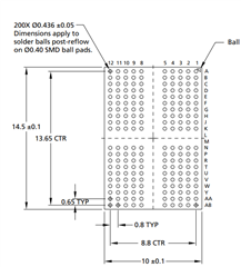
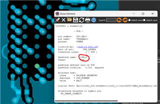
I'm referring to PROC124E2A AM62x-LOW POWER SKEVM, which uses MT53E1G16D1FW-046 WT:A LPDDR4. According to datasheet the size of the solderballs should be 0.436mm and PCB board uses 13mils(0.3302mm). 

Also, if you see the spacing between two pins (0.65-0.436 = 0.214 mm = 8mils). Even if we choose a minimum trace width of 3mils, there is not enough space between the trace and pins. 

Why was the pin diameter reduced and were there any consequences because of this?
Thanks

Santosh

  • Hi Santhosh,


    PCB pad is NSMD and LPDDR4 package pad is SMD, so the PCB pad should be smaller than the Ø0.40 SMD opening on LPDDR4 package. The ratio is 1:0.8 (Pkg SMO: PCB pad)
    With NSMD, the pad can be smaller as solder wets the sides/wall of the pad.
    Note that the raw ball size is Ø0.436mm according to Micron datasheet.

    Refer to https://www.micron.com/content/dam/micron/global/public/products/customer-service-note/csn33-bga-user-guide.pdf
    * Table 3: Examples of Recommended PCB and Package Interconnect Opening Dimensions
    * Printed Circuit Board Design Guidelines (pros and cons)
        - NSMD pads are smaller and offer more space for trace routing than SMD pads
        - SMD solder joints have higher standoff, which makes the joints more robust during shock or drop events

    Consider Board Level Reliability Testing for your end product

    Refer also to IPC publication 7351 Generic Requirements for Surface Mount Design and Land Patterns

    Regards,
    Mark

  • Thank you so much Mark for the detailed explanation.