Other Parts Discussed in Thread: SYSCONFIG
Tool/software:
Hi,
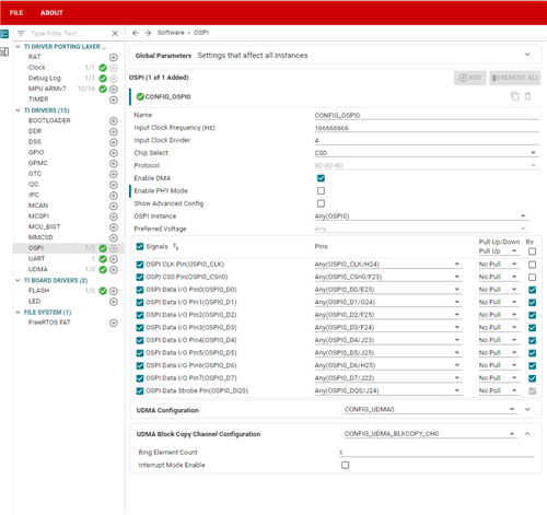
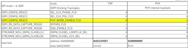
My customer wants to use QSPI PHY mode with internal PHY loopback.
This mode is supported according to the table in original thread. I copied it below.
| PHY | TAP | |||||
| SDR | DDR | SDR | DDR | |||
| reference clock | w/ data training | w/o data training | w/ data training | w/o data training | ||
| No Loopback | NA | NA | NA | NA | 50MHz(Table 7-122) | 25MHz(Table 7-124) |
| Internal PHY Loopback | Not supported | 166MHz or 142MHz (Table 7-116, 7-117) | Not supported | Not supported | NA | NA |
| Internal PAD Loopback | Not supported | Not supported | Not supported | Not supported | NA | NA |
| External Board Loopback | Not supported | 166MHz or 142MHz (Table 7-116, 7-117) | Not supported | 52MHz (Table 7-119, 7-120) | NA | NA |
| DQS | Not supported | Not supported | 166MHz or 132MHz (Table 7-113, 7-114) | 52MHz (Table 7-119, 7-120) | NA | NA |
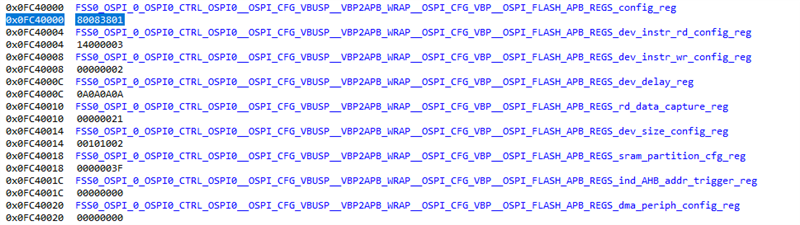
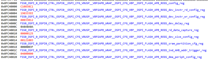
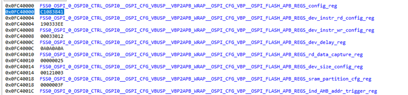
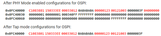
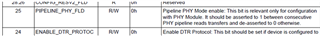
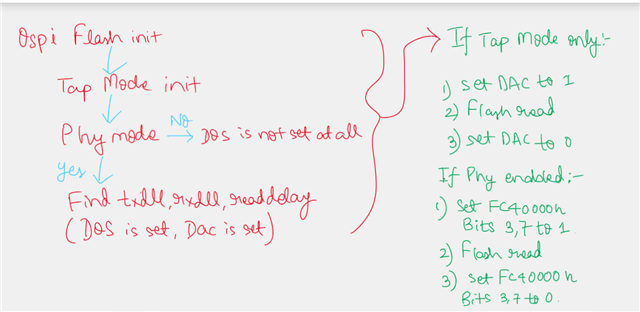
Could you tell me how to configure QSPI registers to enable that mode?
Thanks and regards,
Koichiro Tashiro