This thread has been locked.
If you have a related question, please click the "Ask a related question" button in the top right corner. The newly created question will be automatically linked to this question.
Tool/software:
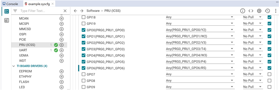
Each PRU_ICSSG PRU processor implements fast GPO through its R30 register and fast GPI through R31 register. AM64x/AM243x has 20 pinned out PRU GPIO pins and the device multiplexes all GPI signals and their corresponding GPO signals onto the same pin using different multiplexing modes.
How to switch between GPO and GPI operation from PRU firmware code?
PRU GPIO Bidirectional mode for AM64x and AM243x
We can program the PRU GPIO pins in bidirectional mode to enable switching between GPO and GPI operation from PRU. Special I/O pin connectivity for the GPO/GPI pins is implemented using the IEP EDIO signal controls to provide input/output switching using a single SoC level pin multiplexing mode.
The IEP EDIO interface has 32 data output enable (DATA_OUT_EN) signals corresponding to its 32 data input and 32 data output signals. On the device, only 4 of the IEP0 EDIO (and none of the IEP1 EDIO) I/Os of each PRU_ICSSG module are pinned out (PRG[2:0]_IEP0_EDIO_DATA_IN_OUT[31:28]).
The unused output enables can be optionally re-purposed as GPO enables allowing each ICSSG GP pin to function as either a GPO or as a GPI when the I/O pin is configured for the GPO muxmode. A set of SoC level registers (CTRLMMR_ICSSG[2:0]_CTRL[2:0]) are used to determine the behavior of each GPO mode pin.
By default, the [19-0]GPM_BIDI bit field is set to 0h and the corresponding GPO pins operate only as an output when the GPO muxmode is selected. The corresponding GPI signal (ICSSG GPI[19:0] input) is driven low.
When a register’s [19-0]GPM_BIDI bit field is set to 1h, the corresponding ICSSG_DIGIO_DATA_OUT_EN_REG[31-0] DATA_OUT_EN bit field is used to control the GPO output buffer.
Steps to enable bidirectional mode in PRU IO Empty project:
Import CCS projects-
Modifications to the R5F project-
Modifications to the PRU project-
Below code enables bidirectional functionality for PRU GPIO[6-0] and converts GPO3 to GPI3. Replace the code present after clearing the register space (zero &r0, 120) in main.asm file with the following.
PIN_CONTROL: ;Unlock CTRLMMR kick protection registers ldi32 TEMP_REG, 0x68EF3490 ldi32 CTRL_REG, 0x43001008 sbbo &TEMP_REG, CTRL_REG, 0, 4 ldi32 TEMP_REG, 0xD172BC5A ldi32 CTRL_REG, 0x4300100C sbbo &TEMP_REG, CTRL_REG, 0, 4 ldi32 TEMP_REG, 0x68EF3490 ldi32 CTRL_REG, 0x43005008 sbbo &TEMP_REG, CTRL_REG, 0, 4 ldi32 TEMP_REG, 0xD172BC5A ldi32 CTRL_REG, 0x4300500C sbbo &TEMP_REG, CTRL_REG, 0, 4
;Set bits 0-6 of CTRLMMR_ICSSG0_CTRL0 to 1 to enable PRU fast GPIO as bidirectional ldi32 TEMP_REG, 0x7F ldi32 CTRL_REG, 0x43004100 sbbo &TEMP_REG, CTRL_REG, 0, 4
;Set bits in IEP_DIGIO_DATA_OUT_EN_REG, GPIO 3 to inputs, rest as outputs ldi32 TEMP_REG, 0x08 ldi32 EN_REG, 0x2e314 sbbo &TEMP_REG, EN_REG, 0, 4 halt ;end of program
Build and run the example-
Follow the steps here - EXAMPLES_PRU_EMPTY to build and run the example
Test the functionality -
Set one of the GPO pins high by writing 1h to the corresponding R30 register bit and externally loop it to GPI3. As a result, value of the R31 register should change on receiving the high signal in GPI3.
Additional Note: Unlocking the CTRLMMR protection mechanism and bidirectional configuration is a one time setup and can be added on R5F side as below.
#define KICK0_UNLOCK_VAL (0x68EF3490U) #define KICK1_UNLOCK_VAL (0xD172BC5AU) #define CSL_MAIN_LOCK0_KICK0_OFFSET (0x1008) #define CSL_MAIN_LOCK1_KICK0_OFFSET (0x5008) void config_CTRLMMR() { uint32_t baseAddr; volatile uint32_t *kickAddr; volatile uint32_t *regAddr = (volatile uint32_t *)((uint32_t)0x43004100); baseAddr = (uint32_t)(0x43000000); /* Lock 0 */ kickAddr = (volatile uint32_t *) (baseAddr + CSL_MAIN_LOCK0_KICK0_OFFSET); CSL_REG32_WR(kickAddr, KICK0_UNLOCK_VAL); /* KICK 0 */ kickAddr++; CSL_REG32_WR(kickAddr, KICK1_UNLOCK_VAL); /* KICK 1 */ /* Lock 1 */ kickAddr = (volatile uint32_t *) (baseAddr + CSL_MAIN_LOCK1_KICK0_OFFSET); CSL_REG32_WR(kickAddr, KICK0_UNLOCK_VAL); /* KICK 0 */ kickAddr++; CSL_REG32_WR(kickAddr, KICK1_UNLOCK_VAL); /* KICK 1 */ CSL_REG32_WR(regAddr, 0x0000007F);
Attached below are the modified PRU IO empty project files with bidirectional mode enabled for PRU GPIO.