This thread has been locked.

If you have a related question, please click the "Ask a related question" button in the top right corner. The newly created question will be automatically linked to this question.

[FAQ] AM625 / AM623 / AM625SIP / AM625-Q1 / AM62A / AM62P Custom board hardware design – CSI-2 capabilities

Part Number: AM625

Tool/software:

Hi TI Experts,

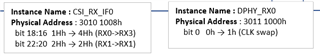
I have the below queries regarding the CSI-2 interface

  1. Supported data rate 
  2. Does the CSI-2 interface provide provision for internal termination 
  3. Links to useful threads 

Let me know your thoughts.

  • Hi Board designers, 

    Refer below inputs for the CSI-2 interface related queries.

    1. Supported data rate 

    Refer to the device specific data sheet. The data rate mentioned is per lane.

          2. Does the CSI-2 interface provide provision for internal termination 

    Provision for internal termination is available.

    3. Does AM62A provide LED flickering mitigation function in its ISP

    LFM is typically handled by image sensors nowadays and there is no special H/W designed in AM62A VPAC (ISP) for LFM.

    4. I see the MIPI_CSI-2 and DSI are all V1.3, can they support DSI v1.2 and CSI V1.2 mode?

    https://e2e.ti.com/support/processors-group/processors/f/processors-forum/1366396/am62p-q1-mipi-interface

    5. I would like to know if MIPI D-PHY of AM62x supports “non-continuous MIPI clock” or “continuous MIPI clock”? Our camera sensor’s clock output is continuous clock. Can AM62x modify MIPI Clock settings via register?

    6. Customer sends camera data through Serdes  interface  to AM62 DPHY RX. can we use AM62 DPHY register to know if  AM62 receives MIPI data correctly?

    The registers we publish for dphy are largely to do with setup like PLL activity and lane mapping. I assume they will use this in conjunction with the CSI which has more registers that indicate bit errors and stream status. This would help understand if things are both configured correctly and functioning. 

    7. Please tell me about swapping the positive and negative of the mipi signal.
    Is it possible to swap mipi's P and N in the same way?
    (ex.W13 RXP0, W12 RXN0 →(swap)→ W12 RXP0, W13 RXN0)

    I was able to successfully emulate frame transmission with the lane remapping configuration:

    DUT Designated Lane CLK-     Remapped Function CLK-

    DUT Designated Lane CLK+     Remapped Function CLK+

    DUT Designated Lane D0-      Remapped Function D3+

    DUT Designated Lane D0+      Remapped Function D3-

    DUT Designated Lane D1-      Remapped Function D1-

    DUT Designated Lane D1+      Remapped Function D1+

    DUT Designated Lane D2-      Remapped Function D0+

    DUT Designated Lane D2+      Remapped Function D0-

    DUT Designated Lane D3-      Remapped Function D2-

    DUT Designated Lane D3+      Remapped Function D2+

    The customer should not encounter any HW problems doing this.

    8. I'm very happy to hear that I can do the MIPI line swap that I wanted to do. I would like to confirm one thing, was it possible to achieve this by changing the settings as shown in the image below? Or did it become possible to replace it by changing other settings?

    I would appreciate it if you could tell me the specific method.

    These would be accurate register modifications for the updated lane mapping:

    • 0x30101008 - CSIRX_STATIC_CFG
      • [30:28] - dl3_map = 0x3
      • [26:24] - dl2_map = 0x1
      • [22:20] - dl1_map = 0x2 (default)
      • [18:16] - dl0_map = 0x4
    • 0x30111000 - DPHYRX_WRAP_LANE
      • [8] - CLK_SWAPDPDN_DL_L_3 = 0x0 (default)
      • [7] - CLK_SWAPDPDN_DL_L_2 = 0x0 (default)
      • [6] - DATA_SWAPDPDN_DL_L_3 = 0x0 (default)
      • [5] - DATA_SWAPDPDN_DL_L_2 = 0x1
      • [4] - CLK_SWAPDPDN_DL_L_1 = 0x0 (default)
      • [3] - CLK_SWAPDPDN_DL_L_0 = 0x0 (default)
      • [2] - DATA_SWAPDPDN_DL_L_1 = 0x0 (default)
      • [1] - DATA_SWAPDPDN_DL_L_0 = 0x1
      • [0] - CLK_SWAPDPDN_DL_L_3 = 0x0 (default)

    Regards,

    Sreenivasa