


Tool/software:
Hello,
I would like to simulate HS200 mode in write phase.
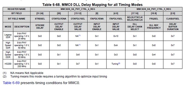
Table 6-68 of the TRM show OTAPDLYSEL is settled to 0x7 that :
What is the corresponding delay value between CLK and others signals?
Thanks for you help.
Original question:

Tool/software:
Hello,
I would like to simulate HS200 mode in write phase.
Table 6-68 of the TRM show OTAPDLYSEL is settled to 0x7 that :
What is the corresponding delay value between CLK and others signals?
Thanks for you help.
